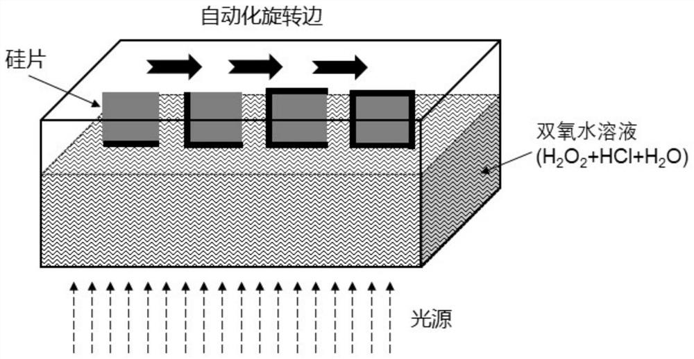
Battery edge passivation method
An edge and battery technology, applied in circuits, electrical components, photovoltaic power generation, etc., can solve the problems of reducing the performance of small cells, increasing the loss of electrical performance, and damage to the edges of small cells, so as to improve photoelectric conversion efficiency, improve power generation performance, The effect of no pollution in the process
- Summary
- Abstract
- Description
- Claims
- Application Information
AI Technical Summary
Problems solved by technology
Method used
Image
Examples
Embodiment 1
[0038] Embodiment 1 discloses a battery edge passivation method, which is used in the preparation process of the battery. This step can be considered to be arranged after the silicon substrate emitter junction is completed, and the front and back coatings (anti-reflection film and passivation film) are prepared. Before, it does not affect the other steps of battery fabrication. Specifically include the following steps:
[0039] A1: After the phosphorus emitter junction (or boron emitter junction) is fabricated on the silicon substrate, the chemical etching process of wet edge removal is used to make the phosphorous silicate glass (or borosilicate glass), oxide layer and emitter junction on the edge of the silicon wafer They are all etched away as completely as possible, so that the silicon at the edge of the silicon substrate is exposed.
[0040] It should be noted that in the present invention, the oxidant needs to react with the exposed silicon on the surface of the crystal...
Embodiment 2
[0045] Embodiment 2 discloses a battery edge passivation method for the battery edge passivation after cutting, which specifically includes the following steps:
[0046] B1: Select a 156 mm*156 mm p-type monocrystalline silicon cell, and laser-cut the cell to form a half-cell (also called a half-cell). Of course, it can also be cut pieces such as one-third, one-quarter, ..., one-Nth, etc.
[0047] B2: The cutting edge of the laser-cut half-chip is contacted with an ozone aqueous solution, and under the condition of photocatalytic oxidation, a silicon oxide film with a thickness of 15 nm is promoted on the exposed silicon surface of the edge of the cell. Among them, the formula of the chemical solution is: 0.57 g / L ozone solution; the solution temperature is 20 °C; the light source can be a dual-spectrum ultraviolet lamp with a power of 150 W, and the wavelengths are ultraviolet light of 185 nm and 254 nm; the time of contact and irradiation is 10 minutes.
[0048] B3: After ...
PUM
| Property | Measurement | Unit |
|---|---|---|
| wavelength | aaaaa | aaaaa |
| thickness | aaaaa | aaaaa |
| thickness | aaaaa | aaaaa |
Abstract
Description
Claims
Application Information
 - R&D
- Intellectual Property
- Life Sciences
- Materials
- Tech Scout
- Unparalleled Data Quality
- Higher Quality Content
- 60% Fewer Hallucinations
Browse by: Latest US Patents, China's latest patents, Technical Efficacy Thesaurus, Application Domain, Technology Topic, Popular Technical Reports.
© 2025 PatSnap. All rights reserved.Legal|Privacy policy|Modern Slavery Act Transparency Statement|Sitemap|About US| Contact US: help@patsnap.com

