


Quick Research
Generate reliable direction feasibility study reports for your R&D in just a few steps.

Technical Q&A
Discover and master advanced knowledge NOW. Basics, ideas, possibilities, all at once.

Find Solutions
As an expert in R&D theories, this can generate solutions to your technical problems instantly.

Evaluate Feasibility
Analyze your overall solution with one click, know your potential R&D risks in advance.

Monitor Landscape
Get weekly tech updates, stay abreast of the latest tech innovations and key insights.
Grooved Field Effect Positive Feedback Transistor Based on Semiconductor Substrate and Fabrication Method
A groove-type, field-effect technology, which is applied in semiconductor/solid-state device manufacturing, semiconductor devices, electrical components, etc., can solve the problem of storage time reduction, increase charge retention time, increase gate oxide layer capacitance, and improve performance. Effect
- Summary
- Abstract
- Description
- Claims
- Application Information
AI Technical Summary
Problems solved by technology
Method used
Image

Examples
Embodiment 1
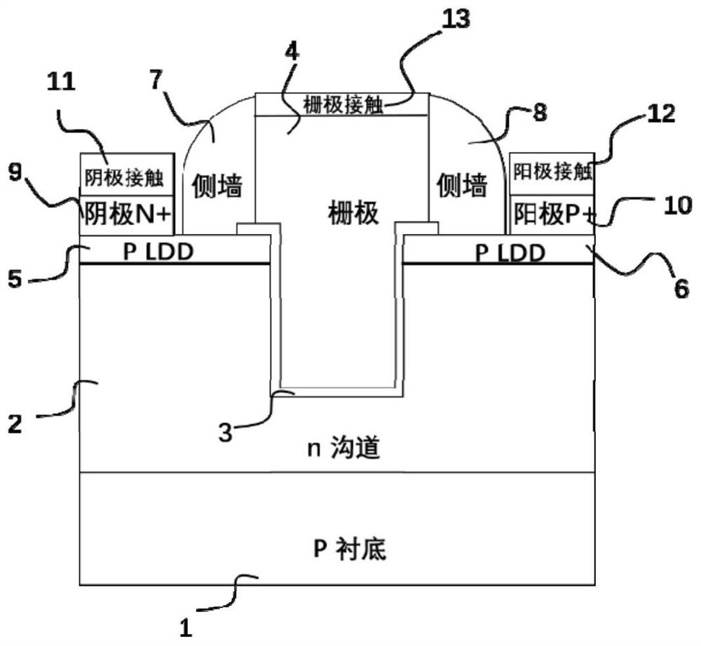
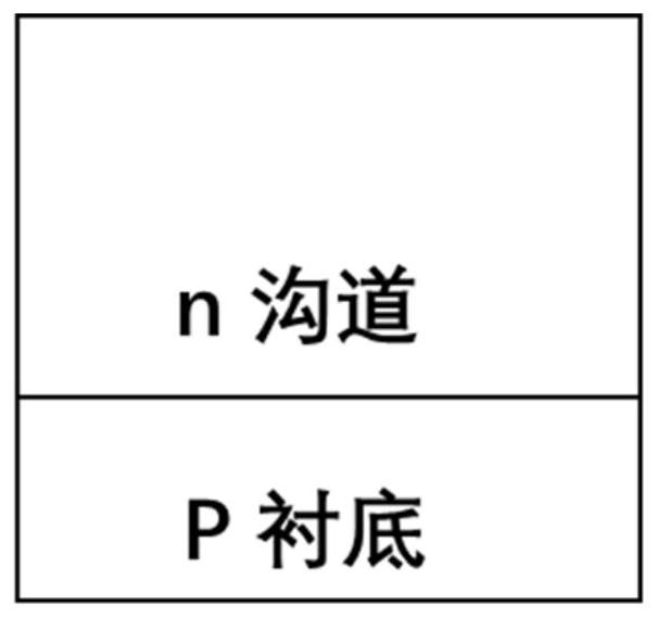
[0104] The substrate 1 is weakly P-doped, the channel region 2 is N-doped, and the low-drain doped region is P-doped. The cathode region 9 is heavily doped with N+ type and the anode region 10 is heavily doped with P+ type.
[0105] In the step S2, the doping concentration of the channel region 2 is 10 15 cm -2 to 10 19 cm -2 Between, the thickness of the channel region 2 is between 50nm and 1000nm.
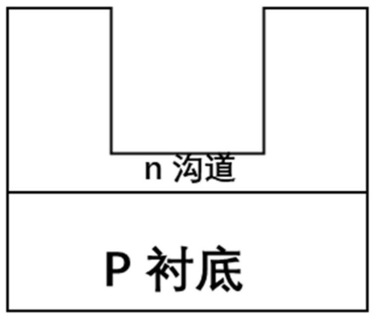
[0106] In the step S3, the etching window of the groove structure is opened by photolithography, and the groove structure is formed by dry etching or wet etching. The dry etching generally uses fluorine-based or halogen gas, such as SF 6 、CHF 3 , HBr or Cl 2 etc. The wet etching generally uses TMAH and KOH solutions, the diameter of the groove structure is generally between 5nm and 200nm, and the depth is generally between 10nm and 1000nm.
[0107] In the step S4, the gate oxide layer 3 is deposited by atomic layer deposition, and the thickness of the gate oxide layer 3 i...
Embodiment 2
[0115] Such as image 3 As shown, the second embodiment is similar to the first embodiment, the difference is that the doping type of the second embodiment is an inverse doping, that is, the device in the second embodiment is a P-type device, and the device in the first embodiment is an N-type device . Wherein the substrate 1 is weakly N-type doped, the channel region 2 is P-type doped, and the ion implantation in the low-drain doped region is N-type doped. The cathode region 9 is doped with N+ type and the anode region 10 is doped with P+ type.
[0116] The specific implementation process flow is similar to the process flow of Example 1. It is only necessary to change the doping of the substrate 1 in step S1 to N-type. In step S6, arsenic or phosphorus is used for ion implantation to form a heavily N-type doped low-drain doped regions with a dose of 10 12 cm -2 to 10 14 cm -2 Between, the energy is between 1keV and 50keV. Others are similar to the first embodiment, and...
Embodiment 3
[0118] Such as Figure 4 As shown, the structure of the third embodiment is similar to the structure of the first embodiment, the difference lies in the formation of the cathode region 9 and the anode region 10 . In the third embodiment, the epitaxy of the cathode region 9 and the anode region 10 does not require in-situ doping and does not require a mask. After epitaxy, N+ and P+ doping is selectively formed in the epitaxial layers of the cathode region 9 and the anode region 10 by combining photolithography and ion implantation.
[0119] A method for preparing the semiconductor substrate-based recessed field effect positive feedback transistor according to this embodiment, the method includes:
[0120] T1. Prepare a weakly doped starting substrate 1 .
[0121] T2. Epitaxially growing a doped channel region 2 on the substrate 1 .
[0122] T3. Using a mask to form a groove structure at a preset position on the channel region 2 .
[0123] T4. Deposit a layer of groove-shape...
PUM
| Property | Measurement | Unit |
|---|---|---|
| thickness | aaaaa | aaaaa |
| diameter | aaaaa | aaaaa |
| depth | aaaaa | aaaaa |
Abstract
Description
Claims
Application Information
 - R&D Engineer
- R&D Manager
- IP Professional
- Industry Leading Data Capabilities
- Powerful AI technology
- Patent DNA Extraction
Browse by: Latest US Patents, China's latest patents, Technical Efficacy Thesaurus, Application Domain, Technology Topic, Popular Technical Reports.
© 2024 PatSnap. All rights reserved.Legal|Privacy policy|Modern Slavery Act Transparency Statement|Sitemap|About US| Contact US: help@patsnap.com