Copper-ceramic interface structure of high-reliability silicon nitride copper-coated ceramic substrate and preparation method of copper-ceramic interface structure

A technology of silicon nitride copper cladding and silicon nitride ceramics, applied in manufacturing tools, welding equipment, metal processing equipment, etc., can solve the problems of affecting the etching process, poor uniformity of copper-ceramic interface, and unclean etching, and avoid environmental problems. Contamination, less stress concentration, uniform welding layer effect

Active Publication Date: 2020-07-10
江苏富乐华半导体科技股份有限公司
View PDF10 Cites 10 Cited by
  • Summary
  • Abstract
  • Description
  • Claims
  • Application Information

AI Technical Summary

Problems solved by technology

[0004] 1. It is not easy to obtain a uniform weld with AgCuTi active metal brazing paste. Usually, AgCuTi solder is coated on the surface of silicon nitride in the form of slurry, and vacuum brazed after sandwiching the copper sheet into a sandwich structure.
Due to the coating thickness of the solder, the flow of the solder after melting, the diffusion of silver in the solder to the copper, and the crystallization of the solder during solidification, the uniformity of the copper-ceramic interface brazed with AgCuTi slurry is poor, such as figure 1 shown
Solder with poor uniformity will affect the subsequent etching process and affect the dimensional accuracy and reliability of the product
[0005] 2. As a heavy metal, Ag in AgCuTi solder will bring the risk of environmental pollution in the subsequent etching process of copper-clad ceramic substrates
[0006] 3. The brazing layer containing silver will affect the accuracy of etching lines, and the silver-containing solder will cause dirty etching and affect the insulation performance of the circuit board
[0007] 4. The electromigration coefficient of silver is relatively large. In the harsh environment, the electromigration of silver in AgCuTi solder will affect the reliability of the product

Method used


Image

  • Copper-ceramic interface structure of high-reliability silicon nitride copper-coated ceramic substrate and preparation method of copper-ceramic interface structure
  • Copper-ceramic interface structure of high-reliability silicon nitride copper-coated ceramic substrate and preparation method of copper-ceramic interface structure
  • Copper-ceramic interface structure of high-reliability silicon nitride copper-coated ceramic substrate and preparation method of copper-ceramic interface structure

Examples


Embodiment 1

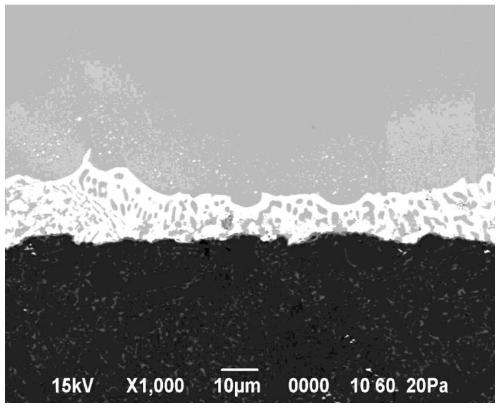
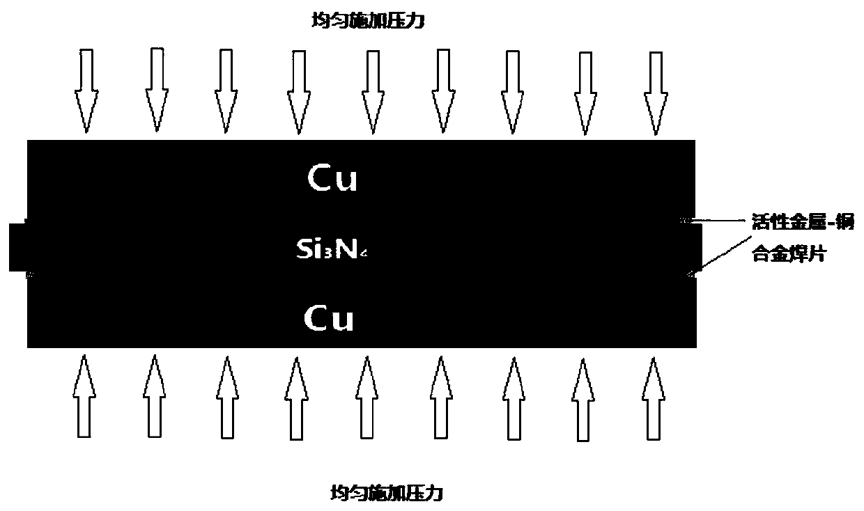
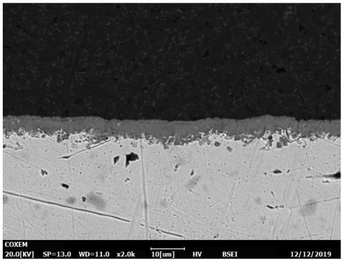
[0037] The invention provides a copper-silicon nitride ceramic connection interface structure for a silicon nitride copper-clad ceramic substrate, the interface structure uses figure 2 The method shown is sintered. The specific implementation method is to use a copper-zirconium alloy sheet with a thickness of 10 microns as a prefabricated welding piece, place it between copper and silicon nitride ceramics, and clamp it into a copper-copper-zirconium alloy welding piece-silicon nitride ceramics-copper zirconium Alloy solder sheet-copper laminated structure, place the laminated structure in the fixture, apply uniform pressure on the copper surface of the laminated structure, the pressure is 1kg / cm 2 . Place the above-mentioned stacked structure in a vacuum sintering furnace to raise the temperature to 980°C at a rate of 10°C / min, keep it warm for 60min, and cool down to room temperature. Wherein, in the copper-zirconium alloy flakes used, the content of active metal element z...

Embodiment 2

[0039]The invention provides a copper-silicon nitride ceramic connection interface structure for a silicon nitride copper-clad ceramic substrate, the interface structure uses figure 2 The method shown is sintered. The specific implementation method is to use a copper-hafnium alloy sheet with a thickness of 20 microns as a prefabricated solder sheet, place it between copper and silicon nitride ceramics, and clamp it into a copper-copper hafnium alloy solder sheet-silicon nitride ceramic-copper hafnium Alloy solder sheet-copper laminated structure, place the laminated structure in the fixture, apply uniform pressure on the copper surface of the laminated structure, the pressure is 0.6kg / cm 2 . Place the above-mentioned stacked structure in a vacuum sintering furnace to raise the temperature to 1060°C at a rate of 10°C / min, keep it warm for 60min, and cool down to room temperature. Wherein, in the copper-hafnium alloy flakes used, the content of the active metal element hafniu...

Embodiment 3

[0041] The invention provides a copper-silicon nitride ceramic connection interface structure for a silicon nitride copper-clad ceramic substrate, the interface structure uses figure 2 The method shown is sintered. The specific implementation method is to use a copper-titanium alloy sheet with a thickness of 5 microns as a prefabricated soldering sheet, place it between copper and silicon nitride ceramics, and clamp it into copper-copper-titanium alloy soldering sheet-silicon nitride ceramics-copper titanium Alloy solder sheet-copper laminated structure, place the laminated structure in the fixture, apply uniform pressure on the copper surface of the laminated structure, the pressure is 0.1kg / cm 2 . The above-mentioned laminated structure was placed in an atmospheric pressure sintering furnace, and the temperature was raised to 1050° C. at a rate of 10° C. / min, kept in an argon atmosphere for 60 minutes, and cooled to room temperature. Wherein, in the copper-titanium alloy ...


PUM

PropertyMeasurementUnit
Thicknessaaaaaaaaaa
Thicknessaaaaaaaaaa
Thermal expansion coefficientaaaaaaaaaa

Abstract

The invention discloses a copper-ceramic interface structure of a high-reliability silicon nitride copper-coated ceramic substrate. The copper-ceramic interface structure comprises copper, a connecting layer, a reaction layer, silicon nitride ceramic, a reaction layer, a connecting layer and copper from top to bottom, the reaction layer is nitride of active metal formed by reaction of active metalelements and silicon nitride, and is used for realizing infiltration and connection of solder, silicon nitride ceramic and copper; the connecting layer is a stress buffer layer for connecting copperand silicon nitride ceramic, and the stress buffer layer is a copper alloy layer of copper and active metal elements; through the optimal design of a welding interface and the use of Ag-free solderinglugs, the uniformity of a welding layer can be effectively improved, and the residual stress between copper-ceramic interfaces is reduced, so that the binding force of the copper-ceramic interfaces is improved, and meanwhile, the risk of environmental pollution is reduced.

Description

technical field [0001] The invention belongs to the field of power semiconductor manufacturing, and in particular relates to a method for designing a copper-ceramic interface of a high-reliability silicon nitride copper-clad ceramic substrate, and is particularly suitable for manufacturing copper-clad ceramic substrates such as semiconductor refrigerators and power semiconductors. Background technique [0002] Silicon nitride copper-clad ceramic substrate is a copper-ceramic composite material formed by silicon nitride ceramics and copper through an active brazing process. It is a new basic material for high-power power electronic circuit structure technology and interconnection technology. The reliability of copper-clad ceramic substrates is closely related to the performance of ceramic materials. Generally, 96% alumina ceramics, aluminum nitride ceramics or zirconia toughened alumina ceramics are used as ceramic materials, but the bending strength and fracture toughness of...

Claims


Application Information

Patent Timeline
IPC IPC(8): H01L23/15H01L21/48B23K1/008B23K35/30
CPCH01L23/15H01L21/4807B23K1/008B23K35/302
Inventor 王斌贺贤汉郭建岳张恩荣马敬伟孙泉
Owner 江苏富乐华半导体科技股份有限公司
Why Eureka
Try Eureka