


Quick Research
Generate reliable direction feasibility study reports for your R&D in just a few steps.

Technical Q&A
Discover and master advanced knowledge NOW. Basics, ideas, possibilities, all at once.

Find Solutions
As an expert in R&D theories, this can generate solutions to your technical problems instantly.

Evaluate Feasibility
Analyze your overall solution with one click, know your potential R&D risks in advance.

Monitor Landscape
Get weekly tech updates, stay abreast of the latest tech innovations and key insights.
Epitaxial structure of Si-based gallium nitride device
An epitaxial structure, gallium nitride technology, applied in the field of microelectronics, can solve problems such as poor lattice quality
- Summary
- Abstract
- Description
- Claims
- Application Information
AI Technical Summary
Problems solved by technology
Method used
Image


Examples
Embodiment 1
[0018] 1. Provide a substrate L1, which is a silicon material used for epitaxial gallium nitride thin film, with a size range of 2-8 inches.
[0019] 2. The nucleation layer L2 is grown by PECVD at a temperature of 500° C., including the AlN layer L21 and the GaN layer L22 , and the total film thickness is 20 nm. Among them, the thickness of the ALN layer L21 is 2nm, the thickness of the GaN layer L22 is 2nm, and the cycle number is 5, see figure 2 .
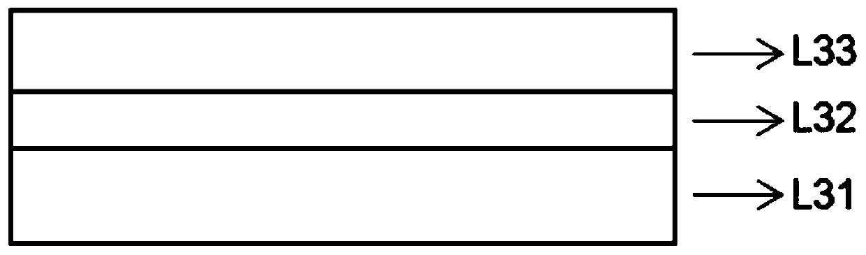
[0020] 3. A buffer layer L3 is grown on the nucleation layer, and its structure is composed of InN / SiN / GaN cyclic growth, including an InN crystal nucleus layer L31, a network structure SiN thin layer L32, and a GaN leveling layer L33. Its growth temperature is 1130°C, and the total thickness of the film is 2um. Among them, the thickness of the InN crystal nucleus layer L31 is 10nm, the thickness of the network structure SiN thin layer L32 is 1nm, the thickness of the GaN leveling layer L33 is 70nm, and the number of cycles i...
Embodiment 2
[0025] 1. Provide a substrate L1, which is a silicon material used for epitaxial gallium nitride thin film, with a size range of 2-8 inches.
[0026] 2. The nucleation layer L2 including the AlN layer L21 and the GaN layer L22 is grown by PECVD at a temperature of 600° C., and the total thickness of the film is 40 nm. Among them, the thickness of the ALN layer L21 is 2nm, the thickness of the GaN layer L22 is 2nm, and the number of cycles is 10, see figure 2 .
[0027] 3. A buffer layer L3 is grown on the nucleation layer, and its structure is composed of InN / SiN / GaN cyclic growth, including an InN crystal nucleus layer L31, a network structure SiN thin layer L32, and a GaN leveling layer L33. Its growth temperature is 1130°C, and the total thickness of the film is 2um. Among them, the thickness of the InN crystal nucleus layer L31 is 10nm, the thickness of the network structure SiN thin layer L32 is 1nm, the thickness of the GaN leveling layer L33 is 70nm, and the number o...
Embodiment 3
[0032] 1. Provide a substrate L1, which is a silicon material used for epitaxial gallium nitride thin film, with a size range of 2-8 inches.
[0033] 2. The nucleation layer L2 is grown by MOCVD at a temperature of 800° C., including the AlN layer L21 and the GaN layer L22 , and the total thickness of the film is 25 nm. Among them, the thickness of the ALN layer L21 is 2nm, the thickness of the GaN layer L22 is 3nm, and the cycle number is between 5, see figure 2 .
[0034] 3. After the core layer is grown, a 10min high-temperature heat treatment is carried out, the temperature is between 1040 and 1070, and the atmosphere is a mixed gas of N2 / H2 / NH3. Continue to grow the buffer layer after heat treatment.
[0035] 4. A buffer layer L3 is grown on the nucleation layer, and its structure is composed of InN / SiN / GaN cyclic growth, including an InN crystal nucleus layer L31, a network structure SiN thin layer L32, and a GaN leveling layer L33. Its growth temperature is 1130°C, ...
PUM
| Property | Measurement | Unit |
|---|---|---|
| Thickness | aaaaa | aaaaa |
| Thickness | aaaaa | aaaaa |
| Thickness | aaaaa | aaaaa |
Abstract
Description
Claims
Application Information
 - R&D Engineer
- R&D Manager
- IP Professional
- Industry Leading Data Capabilities
- Powerful AI technology
- Patent DNA Extraction
Browse by: Latest US Patents, China's latest patents, Technical Efficacy Thesaurus, Application Domain, Technology Topic, Popular Technical Reports.
© 2024 PatSnap. All rights reserved.Legal|Privacy policy|Modern Slavery Act Transparency Statement|Sitemap|About US| Contact US: help@patsnap.com