
Metal oxide semiconductor device and manufacturing method thereof

A technology of oxide semiconductors and production methods, which is applied in the direction of semiconductor/solid-state device manufacturing, transistors, electrical components, etc., to achieve the effects of improving surface potential, facilitating industrialized mass production, and good economic benefits

Active Publication Date: 2021-10-15
SHANGHAI IND U TECH RES INST
View PDF6 Cites 0 Cited by
  • Summary
  • Abstract
  • Description
  • Claims
  • Application Information

AI Technical Summary

Problems solved by technology

In the traditional field effect transistor, C S and C ins are all positive, resulting in (1+C S / C ins ) can never be less than 1, so it cannot be less than 60mV / dec. The negative capacitance effect of ferroelectric materials can make the ferroelectric capacitance negative, that is, C F <0

Method used


Image

  • Metal oxide semiconductor device and manufacturing method thereof
  • Metal oxide semiconductor device and manufacturing method thereof
  • Metal oxide semiconductor device and manufacturing method thereof

Examples


Embodiment 2

[0108] Compared with the first embodiment, the manufacturing method sequence and corresponding process of the metal oxide semiconductor device of the second embodiment are different. The manufacturing method of embodiment two comprises:

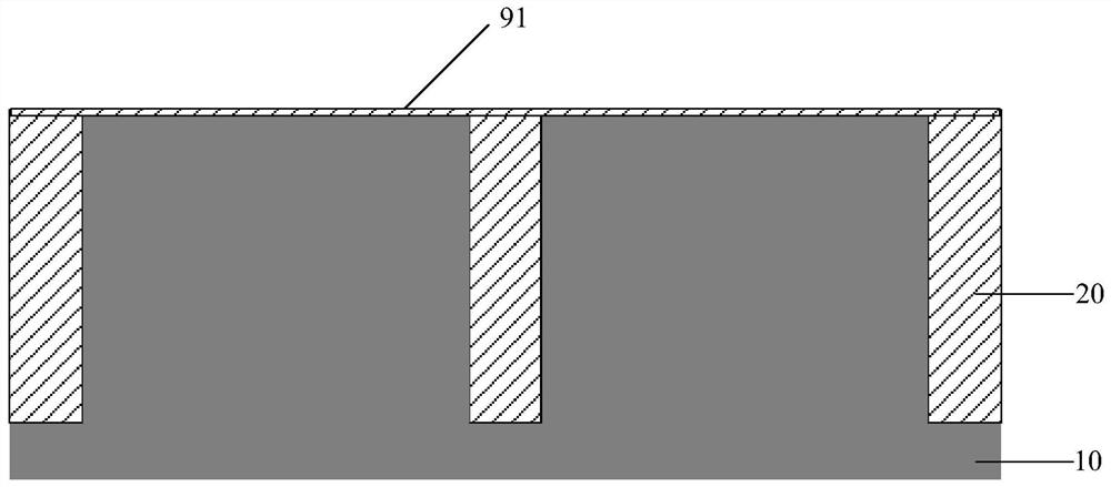
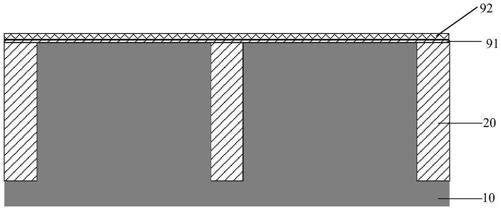
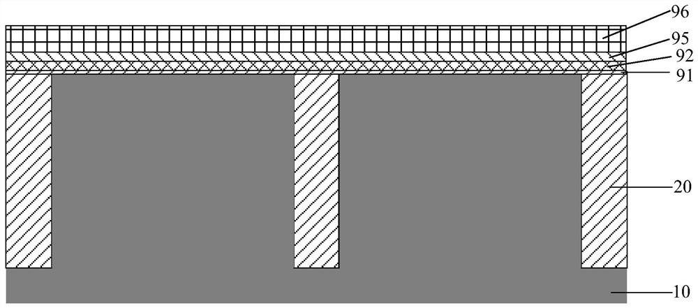
[0109] Step 1: Form the N-type MOSFET region and the P-type MOSFET region separated by the shallow trench isolation region 20 on the substrate 10, form a dummy gate oxide layer 41 and deposit a polysilicon dummy gate 96 thereon; deposit hard mask 30, such as Figure 16 shown.

[0110] Step 2: Photolithography and etching to form a gate stack structure, such as Figure 17 shown.

[0111] Step 3: forming sidewalls 1-71 and N-type and P-type source and drain extension regions 51 and 52; forming sidewalls 2-72 and N + Type and P + Type source and drain regions 53 and 54; form source and drain region silicide 55, such as Figure 18 shown.

[0112] Step 4: Deposit oxide and silicon nitride interlayer dielectric layer 80, and CMP interlayer d...


PUM

PropertyMeasurementUnit
thicknessaaaaaaaaaa
thicknessaaaaaaaaaa
thicknessaaaaaaaaaa

Abstract

The invention discloses a metal oxide semiconductor device and a manufacturing method thereof. The method comprises: forming an N-type MOSFET region and a P-type MOSFET region on a substrate; forming an ultra-thin gate interface oxide layer; forming a ferroelectric material gate dielectric layer, Barrier metal layer and polysilicon dummy gate layer and hard mask; form gate stack structure, gate spacer, N-type and P-type source / drain extension regions and their source / drain regions; deposit oxide and nitride The silicon interlayer dielectric layer is planarized; the first metal gate layer is deposited after removing the dummy polysilicon gate; the first metal gate is doped respectively; and the second metal gate layer is deposited. The metal oxide semiconductor device is finally annealed, which not only makes the interface form a dipole and adjusts the effective work function; but also the clamping effect of the metal electrode during the annealing process induces the generation of ferroelectric negative capacitance effect, which amplifies the surface potential of the channel , resulting in devices with ultra-steep subthreshold slopes and enhanced on / off current ratios.

Description

technical field [0001] The disclosure belongs to the technical field of semiconductors, and relates to a metal oxide semiconductor device and a manufacturing method thereof. Background technique [0002] With the continuous shrinking of the feature size of CMOS devices and the continuous improvement of integration, the power consumption of integrated circuit chips is also increasing. However, because the MOS transistor is based on the hot carrier diffusion conduction mechanism, it cannot overcome the Boltzmann limit, that is, the subthreshold slope (SS) of the device cannot be less than 60mV / dec at room temperature. Limited by the subthreshold swing, if the threshold voltage (V T ), will result in off-state leakage (I OFF ) increases exponentially, so that the leakage power consumption of the device rises linearly. Therefore, the Boltzmann theory limits the operating voltage of the device and cannot be further reduced as the feature size of the device shrinks. Integrated c...

Claims


Application Information

Patent Timeline
Patent Type & Authority Patents(China)
IPC IPC(8): H01L21/8238H01L27/092
Inventor 徐秋霞陈凯
Owner SHANGHAI IND U TECH RES INST
Learn More