A transfer printing method suitable for micro-nano-sized barium titanate thin films
A technology of transfer printing and barium titanate, which is applied in the manufacture of electrical components, circuits, semiconductors/solid-state devices, etc., can solve problems such as difficult barium titanate thin films and single crystal barium titanate integration, and achieve improved graphics accuracy, The bottom surface has good morphology and the effect of reducing the size of the graphics
- Summary
- Abstract
- Description
- Claims
- Application Information
AI Technical Summary
Problems solved by technology
Method used
Image
Examples
Embodiment 1
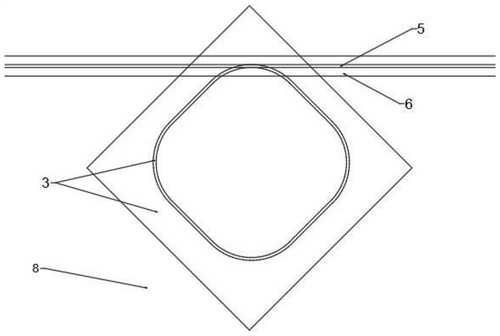
[0038] like figure 2 As shown, the BTO film 3 with a size of 110 μm*110 μm in Embodiment 1 is pasted on the surface of the silicon waveguide covered by BCB after transfer printing.
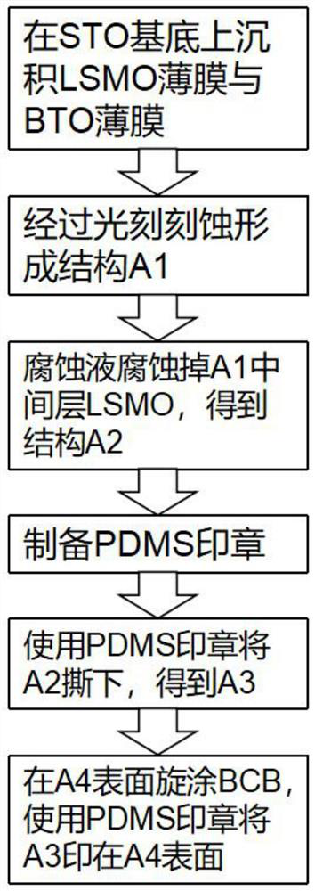
[0039] A transfer printing method suitable for micro-nano size barium titanate (BTO) film, comprising the steps of:
[0040] (1) A LSMO film with a thickness of 200nm was grown on a STO substrate with a thickness of 500μm by pulsed laser deposition, and a BTO film with a thickness of 600nm was grown again,
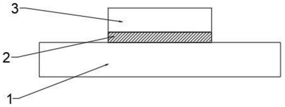
[0041] (2) Use traditional electron beam lithography or deep ultraviolet lithography on the surface of the above-mentioned BTO film 3 to obtain a pattern of 110 μm*110 μm BTO film, and use argon ion etching to bombard the LSMO film layer and the BTO film layer to obtain BTO-LSMO After the second photolithography and development, the structure is formed. The whole structure is marked as A1. The front schematic diagram of the structure is as follows image 3 , where 1 is the STO substrate, 2 ...
Embodiment 2
[0048] like Figure 8 As shown, in Example 2, a strip-shaped BTO thin film 3 with a size of 50 μm*1000 μm was pasted on the surface of the silicon wafer covered by BCB after transfer printing.
[0049] A kind of transfer printing method applicable to micro-nano size barium titanate (BTO) film of the present invention comprises (1) (2) (3) (4) (5) (6) six steps, wherein (1) (3) ) (5) step is the same as in specific example 1. The (2)(4)(6) steps are different from the specific embodiment 1.
[0050] In step (2), a pattern of 50 μm*1000 μm BTO film is obtained by photolithography on the surface of the BTO film 3 using traditional electron beam lithography or deep ultraviolet lithography, and the LSMO layer and the BTO layer are bombarded with argon ion etching to obtain BTO -LSMO column, after the second photolithography and development, the structure A1 is formed;
[0051] In step (4), spin-coat photoresist on a silicon wafer with a thickness of 500 μm and a size of 1.5cm*1....
PUM
| Property | Measurement | Unit |
|---|---|---|
| height | aaaaa | aaaaa |
| thickness | aaaaa | aaaaa |
| thickness | aaaaa | aaaaa |
Abstract
Description
Claims
Application Information
 - R&D
- Intellectual Property
- Life Sciences
- Materials
- Tech Scout
- Unparalleled Data Quality
- Higher Quality Content
- 60% Fewer Hallucinations
Browse by: Latest US Patents, China's latest patents, Technical Efficacy Thesaurus, Application Domain, Technology Topic, Popular Technical Reports.
© 2025 PatSnap. All rights reserved.Legal|Privacy policy|Modern Slavery Act Transparency Statement|Sitemap|About US| Contact US: help@patsnap.com


