Micro-nanostructure controlled copper-based superhydrophobic surface and preparation method and application thereof
A technology of super-hydrophobic surface and micro-nano structure, which is applied in the field of super-hydrophobic surface materials and its preparation, can solve problems such as difficulty in adapting to customized requirements, increased economic costs, and operational complexity, and achieves convenient batch preparation, simple operation, and economical good sex effect
- Summary
- Abstract
- Description
- Claims
- Application Information
AI Technical Summary
Problems solved by technology
Method used
Image
Examples
preparation example Construction
[0041] The preparation process conditions of the copper-based superhydrophobic surface of the present invention are further described below.
[0042] 1. Control the micron structure through laser process parameters.
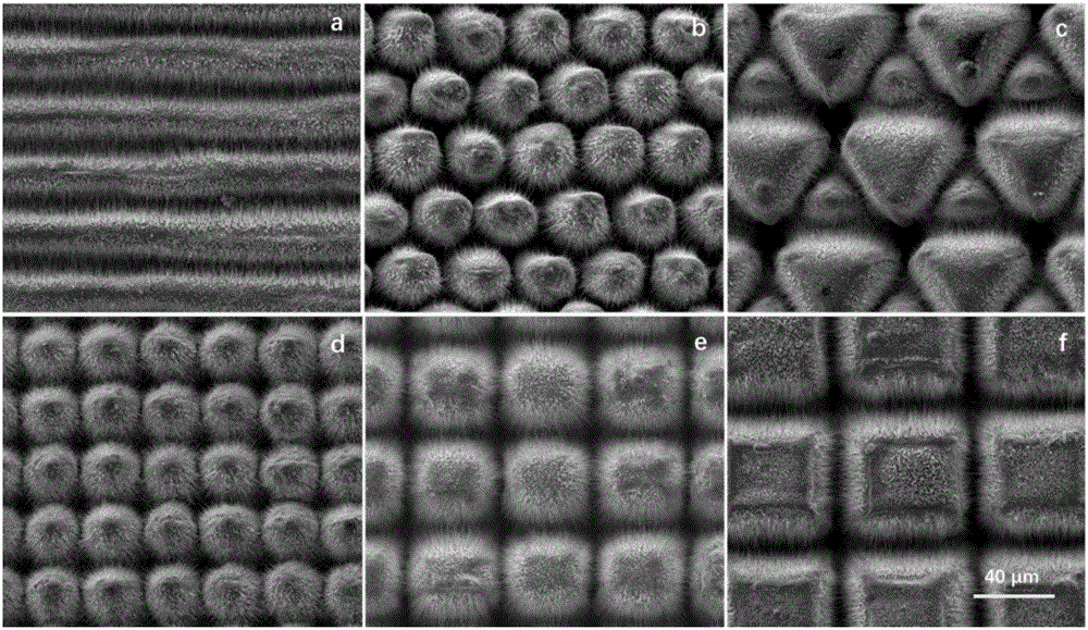
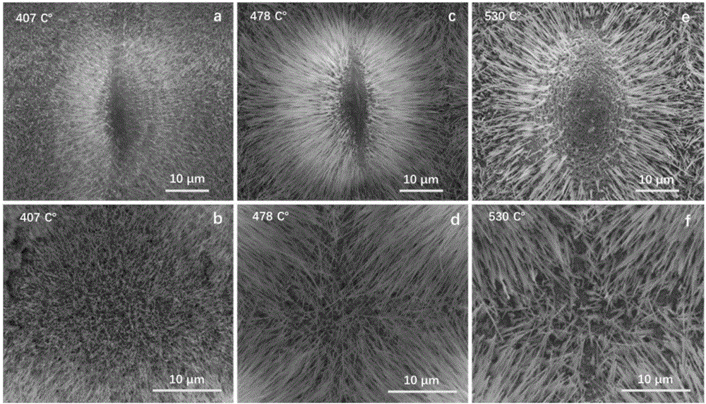
[0043] A computer-aided drawing system is used to control the laser scanning path to obtain patterns with different micron geometric features. The micron structure of the array unit can be hill-shaped, square, triangular, groove, etc.; the arrangement form can be square array, triangular array , strip grooves, etc., the center spacing is 10-500 μm, and the height is 5-500 μm. Then, thermal oxidation treatment is performed on these microstructure surfaces to obtain micronanostructure surfaces with different microstructure basic shapes. During the steam condensation process, the condensing surface with different morphological characteristics has different control effects on the condensed droplets. Therefore, the microstructure can be customized according to the d...
Embodiment
[0064] Example A method for preparing a copper-based superhydrophobic surface with controllable micro-nano structure
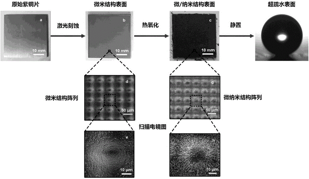
[0065] This embodiment provides a method for preparing a copper-based superhydrophobic surface with controllable micro-nano structure, such as figure 1 As shown, the steps are as follows:
[0066] (1) Surface pretreatment. The copper sheet (purity 99.9%, size 40×40×2mm 3 ) was polished with 2000-grit sandpaper, and then the sample was ultrasonically cleaned in acetone for 10 minutes. After taking it out, it was washed with isopropanol, ethanol and deionized water in sequence, and dried with nitrogen.
[0067] (2) Laser etching. Adopt Edgewave PX100intelliSCANSe14 picosecond laser, the laser center wavelength is 1064nm, the repetition frequency is 597.44KHz, the full power is 60% (full power is 65.4W), the focal length of the galvanometer is 100mm, the array spacing is 55μm, and the scanning speed is 3m / s. The number of repetitions is 30 times, and the sur...
PUM
| Property | Measurement | Unit |
|---|---|---|
| height | aaaaa | aaaaa |
| diameter | aaaaa | aaaaa |
| length | aaaaa | aaaaa |
Abstract
Description
Claims
Application Information
 - R&D Engineer
- R&D Manager
- IP Professional
- Industry Leading Data Capabilities
- Powerful AI technology
- Patent DNA Extraction
Browse by: Latest US Patents, China's latest patents, Technical Efficacy Thesaurus, Application Domain, Technology Topic, Popular Technical Reports.
© 2024 PatSnap. All rights reserved.Legal|Privacy policy|Modern Slavery Act Transparency Statement|Sitemap|About US| Contact US: help@patsnap.com


