Tunable laser and preparation method thereof
A technology for tuning lasers and grating regions, used in lasers, laser components, semiconductor lasers, etc., can solve the problems of weak electronic confinement, small temperature range of devices, and reduced modulation bandwidth, and achieve good electronic confinement. Loss of light, effect of reducing light loss
- Summary
- Abstract
- Description
- Claims
- Application Information
AI Technical Summary
Problems solved by technology
Method used
Image
Examples
preparation example Construction
[0044] The present invention also proposes a method for preparing a tunable laser, including the following steps: Step 1, growing a lower waveguide layer, an active layer of a multi-quantum well structure, and an upper waveguide layer on a substrate in sequence, wherein the main body of the active layer The material is an InGaAlAs quaternary compound; step 2, remove the lower waveguide layer in some areas, the active region and the upper waveguide layer of the multi-quantum well structure, and expose the substrate, so that the structure in step 1 is divided into a gain region and a passive region. Part; step 3, corroding the sidewall of the gain region close to the passive region to form a slope; step 4, growing InGaAsP / InGaAlAs quaternary compound material in the passive region by using butt growth technology, so as to be flush with the upper waveguide layer of the gain region; And a grating structure is prepared in a part of the passive area far away from the gain area, so th...
Embodiment
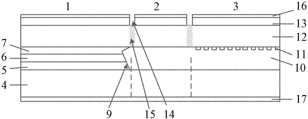
[0067] Such as figure 1 As shown, this embodiment proposes a tunable laser, including a gain region 1, a phase region 2, and a grating region 3 that are located on the same substrate 4, have the same height and are sequentially attached, wherein: the gain region 1 is from bottom to top Include in sequence: a lower waveguide layer 5, an active layer 6 and an upper waveguide layer 7, the active layer 6 is a multi-quantum well structure, the multi-quantum well structure includes 5 well layers and 6 barrier layers stacked alternately, the well layer The main materials of the barrier layer and the barrier layer are all InGaAlAs quaternary compounds; the side surfaces of the lower waveguide layer 5, the active region 6 and the upper waveguide layer 7 near the phase region are etched to form a slope 9; the phase region 2 and the grating region 3 include no The source layer 10 and the passive layer 10 of the grating area 3 are formed with a grating structure 11; the side of the phase ...
PUM
| Property | Measurement | Unit |
|---|---|---|
| Thickness | aaaaa | aaaaa |
| Thickness | aaaaa | aaaaa |
| Thickness | aaaaa | aaaaa |
Abstract
Description
Claims
Application Information
 - Generate Ideas
- Intellectual Property
- Life Sciences
- Materials
- Tech Scout
- Unparalleled Data Quality
- Higher Quality Content
- 60% Fewer Hallucinations
Browse by: Latest US Patents, China's latest patents, Technical Efficacy Thesaurus, Application Domain, Technology Topic, Popular Technical Reports.
© 2025 PatSnap. All rights reserved.Legal|Privacy policy|Modern Slavery Act Transparency Statement|Sitemap|About US| Contact US: help@patsnap.com


