PERC solar cell structure and preparation process thereof
A solar cell and preparation technology, applied in the direction of sustainable manufacturing/processing, circuits, photovoltaic power generation, etc., can solve the problems of LID light-induced attenuation increase, pollution, hidden cracks, etc., to increase process complexity, enrich hydrogen sources, The effect of preventing leakage
- Summary
- Abstract
- Description
- Claims
- Application Information
AI Technical Summary
Problems solved by technology
Method used
Image
Examples
Embodiment 1
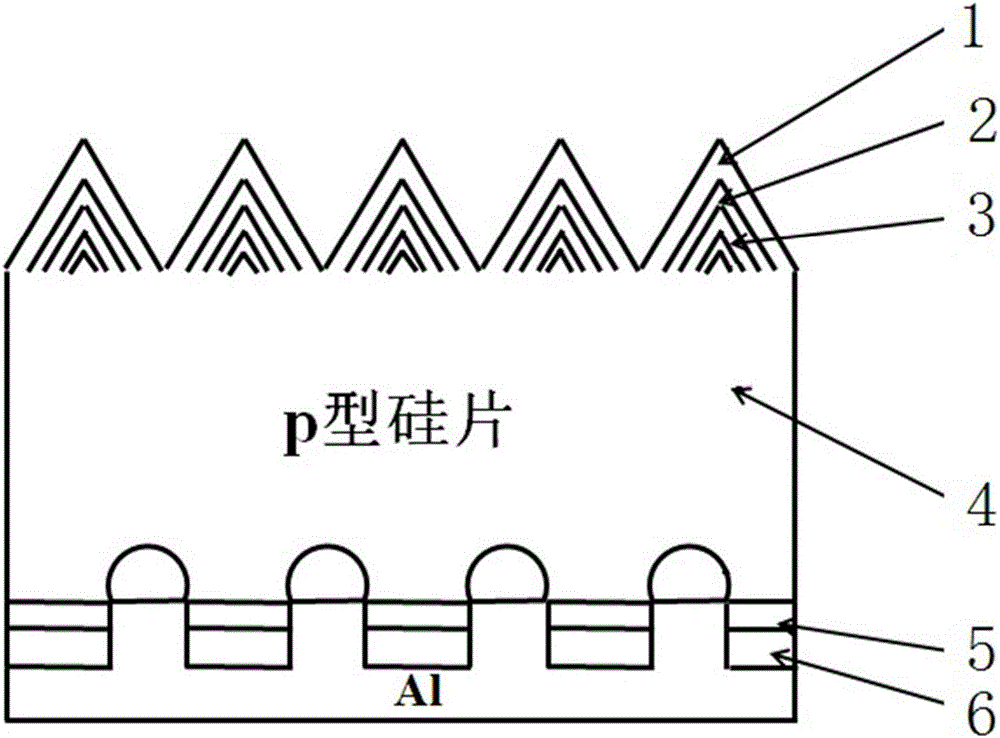
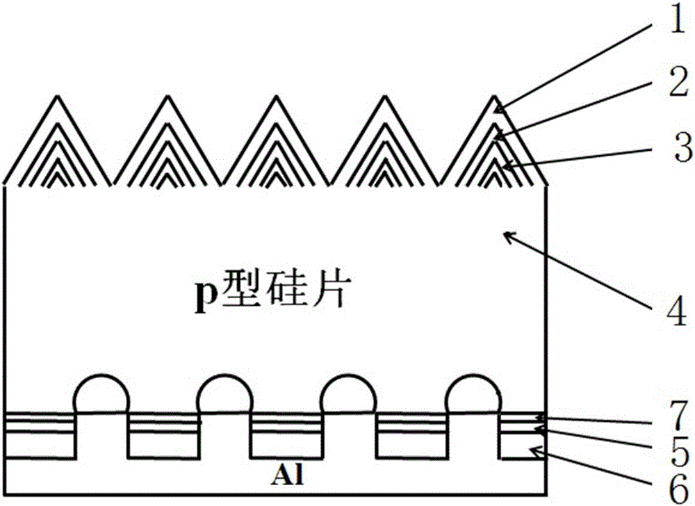
[0047] 1. Silicon wafers in alkaline (NaOH or KOH) or acidic solution (HF+HNO 3 ) after velvet making, wash, dry, and the velvet surface size is within 5um;
[0048] 2. Diffusion of high-temperature phosphorus is carried out in the diffusion furnace, the diffusion resistance is 80Ω / □, and the surface concentration is 6*10 20 atom / cm 3 , the junction depth is 300nm, after forming the pn junction, perform wet etching to remove the back junction and PSG;
[0049] 3. Oxidation is carried out in a high-temperature furnace at a temperature of 750°C and an oxidation time of 15 minutes. After oxidation, the surface concentration is 1.5*10 20 atom / cm 3 , the junction depth is 400nm; the temperature inside the tube is 750°C, and POCl 3 , the oxide layer is doped with impurities for 300s. After doping, the surface concentration is 5*10 20 atom / cm 3 ;
[0050] 4. Deposit the anti-reflection layer on the front side, using PECVD (introducing SiH 4 , NH 3 and N 2 O) depositing a Si...
Embodiment 2
[0057] In Example 1, in step 2, the diffusion resistance is 100Ω / □, and the surface concentration is 3*10 20 atom / cm 3 , the junction depth is 200nm, after the pn junction is formed, wet etching is performed to remove the back junction and PSG; the third step is to oxidize in a high-temperature furnace at a temperature of 750°C, and the oxidation time is 15min. After oxidation, the surface concentration is 9*10 19 atom / cm 3 , the junction depth is 300nm; the temperature inside the tube rises to 800°C, and POCl 3 , the oxide layer is doped with impurities for 300s. After doping, the surface concentration is 5*10 20 atom / cm 3 ; Other processes are the same as in Example 1.
Embodiment 3
[0059] In embodiment 1, in the 4th step, adopt PECVD (feed into SiH 4 , NH 3 and N 2 O) Deposit SiNx / SiOxNy / SiOx laminated structure on the emission area, SiNx refractive index is 2.2, film thickness is 5nm, SiOxNy refractive index is 1.9, film thickness is 30nm, SiOx refractive index is 1.6, film thickness is 40nm; Other Process is identical with embodiment 1.
PUM
 Abstract
Description
Claims
Application Information
 - R&D
- Intellectual Property
- Life Sciences
- Materials
- Tech Scout
- Unparalleled Data Quality
- Higher Quality Content
- 60% Fewer Hallucinations
Browse by: Latest US Patents, China's latest patents, Technical Efficacy Thesaurus, Application Domain, Technology Topic, Popular Technical Reports.
© 2025 PatSnap. All rights reserved.Legal|Privacy policy|Modern Slavery Act Transparency Statement|Sitemap|About US| Contact US: help@patsnap.com


