Perovskite solar battery and preparation method thereof
A solar cell and perovskite technology, applied in the field of solar cells, achieves the effects of good repeatability, high efficiency, and a simple and convenient method
- Summary
- Abstract
- Description
- Claims
- Application Information
AI Technical Summary
Problems solved by technology
Method used
Image
Examples
Embodiment 1
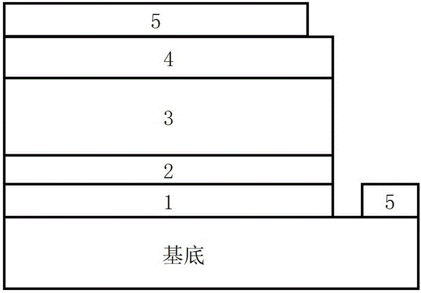
[0023] See attached figure 1 , which is a structural schematic diagram of a perovskite solar cell provided by the present invention, which includes a rigid glass substrate, a cathode 1, an electron transport layer 2, a perovskite light-absorbing layer 3, a hole transport layer 4 and an anode 5, the device The preparation method comprises the steps:
[0024] Step 1, cleaning the cathode 1 composed of the glass substrate and the transparent electrode with acetone, detergent, isopropanol and acetone respectively. After the substrate was treated with ultraviolet ozone for 20 minutes, at room temperature, a niobium oxide film was prepared by magnetron sputtering to form an electron transport layer 2 for transporting electrons: RF sputtering, the power was 150 watts, and the distance between the target and the sample was 15 cm to form a 150 nm niobium oxide electron transport layer 2 . The work function of the niobium oxide thin film measured by ultraviolet photoelectron spectrosc...
Embodiment 2
[0029] This embodiment provides a kind of perovskite solar cell, its structure is as follows figure 1 As shown, the specific preparation steps are as follows:
[0030] Step 1, cleaning the cathode 1 composed of the glass substrate and the transparent electrode with acetone, detergent, isopropanol and acetone respectively. After applying ultraviolet ozone to the substrate for 20 minutes, magnetron sputtering was used at room temperature to prepare a niobium oxide film to form an electron transport layer for transporting electrons 2: radio frequency sputtering, the power is 100 watts, and the distance between the target and the sample is 15 cm, forming 100 nm niobium oxide electron transport layer 2 .
[0031] Step 2, anneal the prepared niobium oxide electron transport layer 2 in air at 500°C for 45 minutes to obtain hexagonal niobium oxide, and use ultraviolet ozone for 10 minutes to prepare perovskite light-absorbing layer 3 on the electron transport layer 2 by spin coating ...
Embodiment 3
[0035] This embodiment provides a figure 1 The preparation method of the shown perovskite solar cell uses a flexible substrate, and the specific steps are as follows:
[0036] In step 1, the cathode 1 composed of polyethylene terephthalate (PET) and the transparent electrode is cleaned with acetone, detergent, isopropanol and acetone respectively. After the substrate was treated with ultraviolet ozone for 20 minutes, a niobium oxide film was prepared by magnetron sputtering at room temperature to form an electron transport layer for transporting electrons 2: RF sputtering, the power is 50 watts, and the distance between the target and the sample is 15 cm , forming a 50 nm niobium oxide electron transport layer 2 .
[0037] Step 2, the substrate is treated with ultraviolet ozone for 10 minutes, and the perovskite light-absorbing layer 3 is prepared by spin coating on the electron transport layer 2. The specific method is to use lead iodide and methylamino iodide in a molar rat...
PUM
| Property | Measurement | Unit |
|---|---|---|
| thickness | aaaaa | aaaaa |
| electron work function | aaaaa | aaaaa |
| thickness | aaaaa | aaaaa |
Abstract
Description
Claims
Application Information
 - Generate Ideas
- Intellectual Property
- Life Sciences
- Materials
- Tech Scout
- Unparalleled Data Quality
- Higher Quality Content
- 60% Fewer Hallucinations
Browse by: Latest US Patents, China's latest patents, Technical Efficacy Thesaurus, Application Domain, Technology Topic, Popular Technical Reports.
© 2025 PatSnap. All rights reserved.Legal|Privacy policy|Modern Slavery Act Transparency Statement|Sitemap|About US| Contact US: help@patsnap.com


