Wafer-Supporting Device and Method for Producing Same

Active Publication Date: 2013-01-17
ASM JAPAN
View PDF60 Cites 317 Cited by
  • Summary
  • Abstract
  • Description
  • Claims
  • Application Information

AI Technical Summary

Benefits of technology

The present invention provides a wafer-supporting device that reduces the number of particles attached to the reverse side of a wafer during film formation and improves film properties such as film stress and uniformity of film thickness. This is achieved by designing a susceptor top surface with protrusions having rounded tips that reduce the contact area between the reverse side of a wafer and the top surface of the device. Additionally, by controlling the number and height of the protrusions, film stress can be minimized while still reducing the accumulation of particles on the reverse side of the wafer.

Problems solved by technology

Further, depending on the type of processing, sticking of the reverse side of a wafer on the top surface of the wafer-supporting device often happens.
However, even when the emboss type or dimple type wafer-supporting device is used, generation and accumulation of particles on the reverse side of a wafer are still a problem.
Further, the convex or concave portions of the wafer-supporting device also affect uniformity of film thickness and film properties.
However, when the number of protrusions is small, a wafer tends to undergo slight sagging or deformation between the contact points (even if it is a small degree) depending on the type of processing, thereby contacting the top surface of the susceptor and increasing generation and accumulation of particles on the reverse side of the wafer.
However, when the height of the protrusions is increased, film stress tends to suffer.

Method used


Image

  • Wafer-Supporting Device and Method for Producing Same
  • Wafer-Supporting Device and Method for Producing Same
  • Wafer-Supporting Device and Method for Producing Same

Examples


example 1

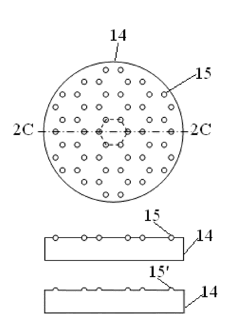
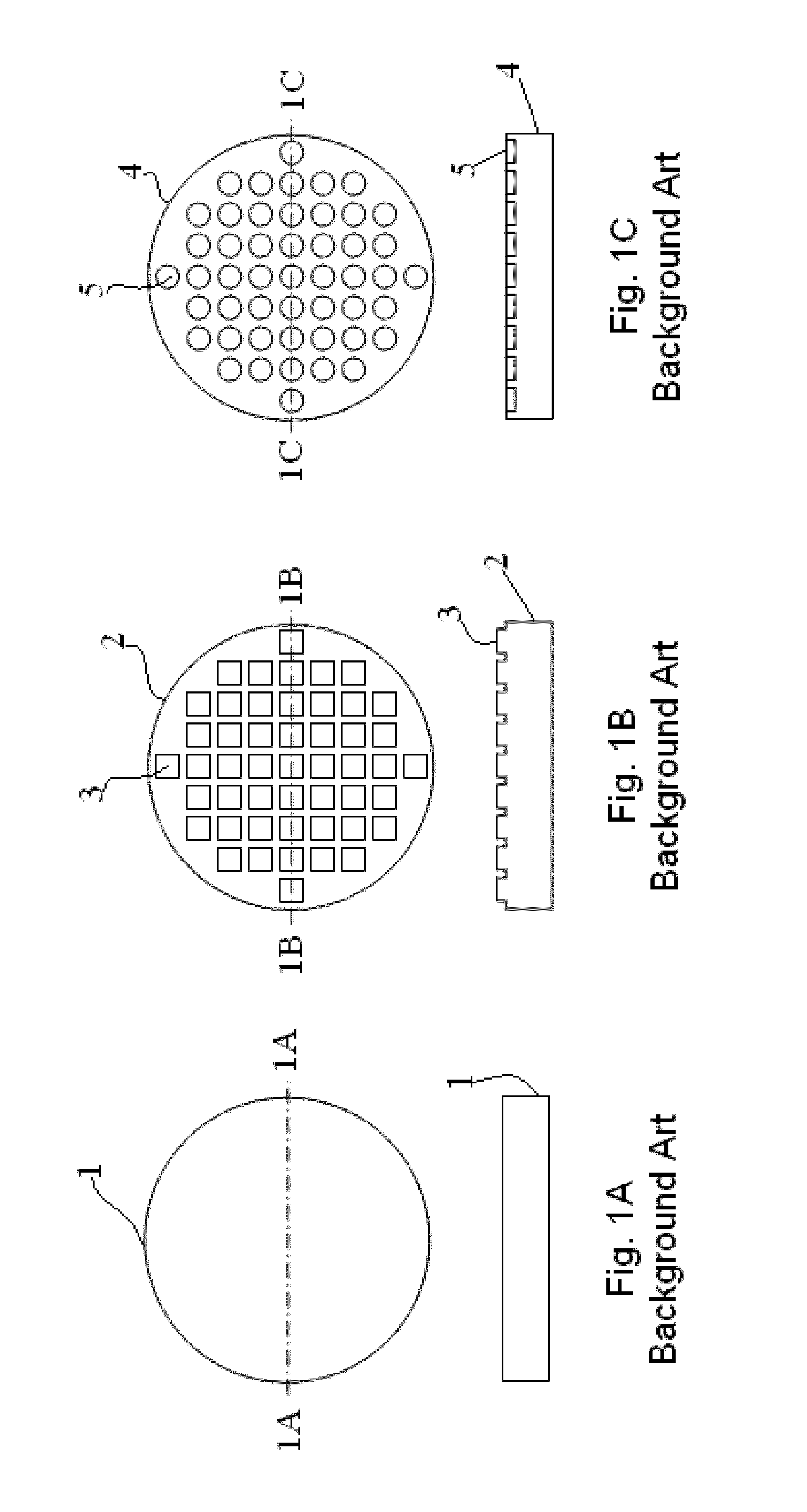
[0062]Film formation was conducted on a wafer in the same manner as in Comparative Example 1, except that a wafer-supporting device illustrated in FIG. 2B (37 protrusions) using sapphire balls having a diameter of 2 mm and a height (H′) of 50 μm (H=38 μm) was used. Due to the differences in thermal expansion coefficient between the aluminum alloy body and the sapphire balls, the height in use (H) was determined to be about 12 μm shorter than the height in non-use (H′) as calculated below:

A=CTE(M)(23E−6: aluminum alloy 6061)×D(M)(0.002 m)×(T1−T0)(T1=390° C., T0=25° C.)=17.0E−6 m

B=CTE(B)(7E−6: aluminum alloy 6061)×D(M)(0.002 m)×(T1−T0)(T1=390° C., T0=25° C.)=5.18E−6 m

A−B=11.8E−6 m

H=H′−11.8 [μm] (≈12 μm).

[0063]FIG. 4 is an image of Defect Review SEM (scanning electron microscope) of a scratched portion of the reverse side of the wafer after the film formation. FIG. 5 is an image of Defect Review SEM (scanning electron microscope) of a circular deformation portion of the reverse side of...

example 2

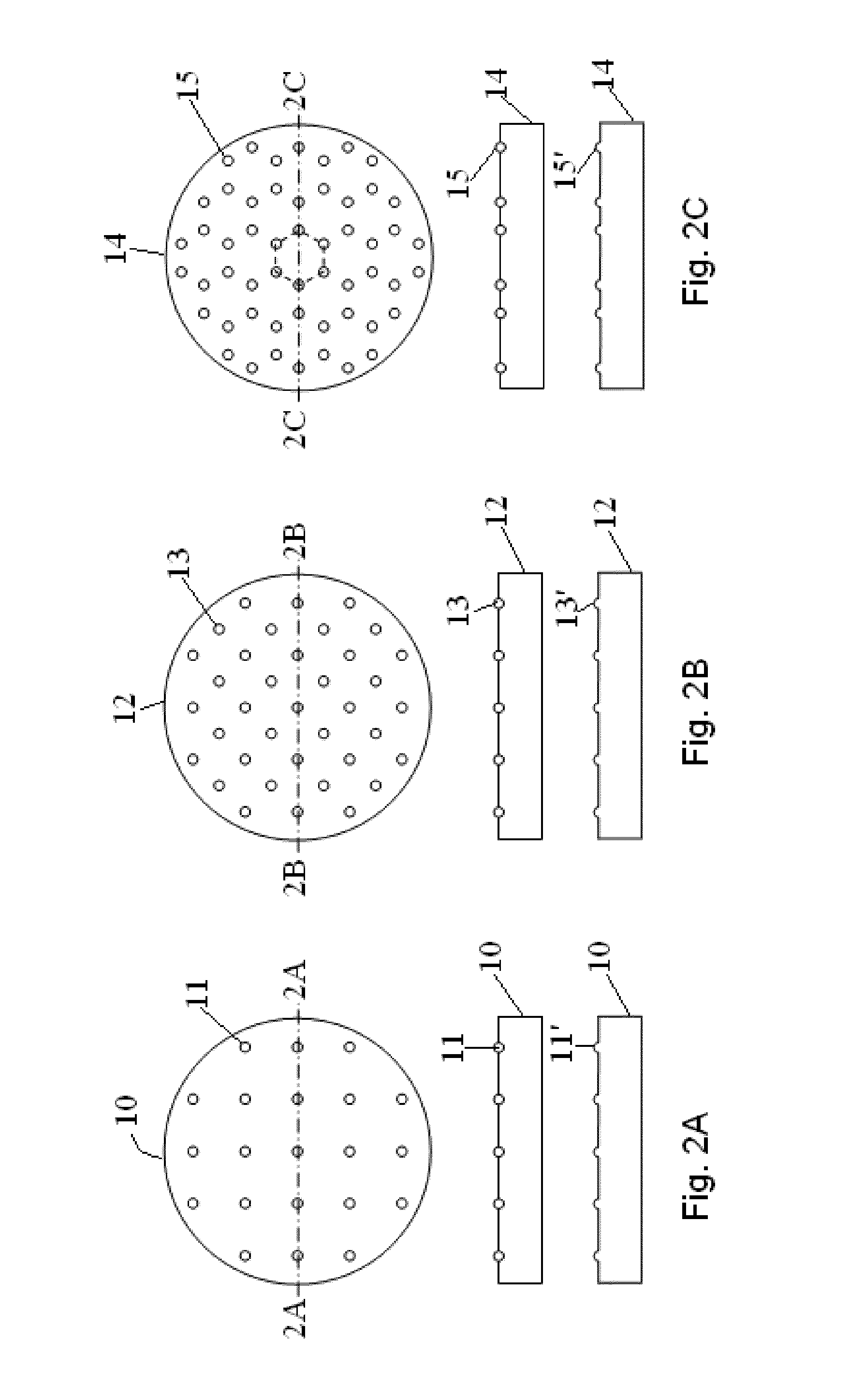
[0064]Film formation was conducted on a wafer in the same manner as in Example 1, except that a wafer-supporting device illustrated in FIG. 2A (21 protrusions) using sapphire balls having a diameter of 2 mm, and a wafer-supporting device illustrated in FIG. 2B (37 protrusions) using sapphire balls having a diameter of 2 mm were used, and the height (H′) of these wafer-supporting devices was changed as shown in FIG. 8, and film stress of the films was measured (due to the differences in thermal expansion coefficient between the aluminum alloy body and the sapphire balls, the height in use (H) was determined to be about 12 μm shorter than the height in non-use (H′)). FIG. 8 is a graph illustrating the relationship between the film stress and the height (H′) of protrusions according to this embodiment. The stress was the average of seven films, and the data when the height (H′) was 40 μm or less were obtained using the wafer-supporting device illustrated in FIG. 2A, and the data when t...

example 3

[0065]Film formation was conducted on a wafer in the same manner as in Example 1, except that a wafer-supporting device illustrated in FIG. 2A (21 protrusions) using sapphire balls having a diameter of 2 mm, and a wafer-supporting device illustrated in FIG. 2B (37 protrusions) using sapphire balls having a diameter of 2 mm were used, and the height (H′) of these wafer-supporting devices was changed as shown in FIG. 9, and the number of particles on the reverse side of the wafer was measured. FIG. 9 is a graph illustrating the relationship between the number of particles on a reverse side of a wafer and the height (H′) of protrusions according to this embodiment. The number of particles was the average of three wafers. As shown in FIG. 9, when the height (H′) of the protrusions illustrated in FIG. 2A (21 protrusions) was no less than about 40 μm (H about 28 μm), the number of particles having a diameter of 0.2 μm or larger could be controlled to under about 300, whereas when the heig...


PUM

PropertyMeasurementUnit
Diameteraaaaaaaaaa
Diameteraaaaaaaaaa
Lengthaaaaaaaaaa

Abstract

A wafer-supporting device for supporting a wafer thereon adapted to be installed in a semiconductor-processing apparatus includes: a base surface; and protrusions protruding from the base surface and having rounded tips for supporting a wafer thereon. The rounded tips are such that a reverse side of a wafer is supported entirely by the rounded tips by point contact. The protrusions are disposed substantially uniformly on an area of the base surface over which a wafer is placed, wherein the number (N) and the height (H [μm]) of the protrusions as determined in use satisfy the following inequities per area for a 300-mm wafer:(−0.5N+40)≦H≦53; 5≦N<100.

Description

BACKGROUND[0001]1. Field of the Invention[0002]The present invention generally relates to a wafer-supporting device installed in a semiconductor-processing chamber, particularly to a wafer-supporting device having protrusions for supporting a wafer thereon.[0003]2. Description of the Related Art[0004]One typical conventional susceptor has a flat surface as shown in FIG. 1A. A wafer-supporting device 1 is adapted to be attached to a susceptor base which typically includes a heater. A wafer is placed on the wafer-supporting device for processing typically by plasma enhanced CVD or ALD. As shown in FIG. 1A (the top figure is a plan view, and the bottom figure is a cross section view taken along line 1A-1A), the wafer-supporting device has a flat surface. However, when a wafer is placed on the flat surface and processed, generation and accumulation of particles are typically observed on a reverse side of the wafer after film formation. Further, depending on the type of processing, stick...

Claims


Application Information

Patent Timeline
IPC IPC(8): B05C13/00C23C16/458B05D5/00H01L21/3065
CPCC23C16/402C23C16/4581H01L21/6875C23C16/5096C23C16/4583
Inventor SHOJI, FUMITAKAFUKUDA, HIDEAKI
Owner ASM JAPAN
Why Eureka
Try Eureka