A polymer photobleaching optical waveguide and microfluidic plate-free integrated chip and its preparation method

An integrated chip and microfluidic technology, applied in the direction of optical waveguide light guide, light guide, optomechanical equipment, etc., can solve the problems of increasing process cost, complicated process, and restricting the development of optical waveguide microfluidic integrated chip, so as to avoid plate alignment error, reducing the effects of bending loss and scattering loss

Active Publication Date: 2018-10-02
JILIN UNIV
View PDF6 Cites 0 Cited by
  • Summary
  • Abstract
  • Description
  • Claims
  • Application Information

AI Technical Summary

Problems solved by technology

The length of the sensing window will affect the sensing accuracy of the device. The increase of the sensing window length will improve the sensing accuracy, but the increase of the sensing window length will also increase the error of the double-layer chip alignment of the optical waveguide and the microfluidic channel. The influence of device precision, this kind of error caused by double-layer chip alignment is unavoidable, which restricts the development of optical waveguide microfluidic integrated chips
[0004] The existing process problems are summarized as follows: 1. Optical waveguides and microfluidic three-dimensional integrated devices need to prepare optical waveguides first, spin-coat cladding, and then prepare sensing windows by means of plate alignment, photolithography, masking, and etching. The process is complicated, the plate registration error cannot be avoided, and the scattering caused by the etching of the sensing window will affect the optical performance of the optical waveguide
2. In the optical waveguide microfluidic three-dimensional integrated structure, the lower layer waveguide usually adopts an inverted ridge structure with exposed surface, and the waveguide device of this structure loses a lot when it is bent; if the flat layer of the inverted ridge structure is removed by etching, the surface layer is formed Exposed rectangular structure, the loss caused by etching affects the optical performance of the optical waveguide
3. The process of optical waveguide and microfluidic chip packaging is complicated, and UV glue or plasma treatment is usually used to bond and bond. UV liquid glue is easy to block the channel and sensing window, and plasma treatment will increase the scattering loss of the optical waveguide in the sensing area , and increase the process cost
4 After the samples are bonded, the size and thickness of the multi-layer samples are larger than the cutting range of the dicing machine, and the end surface treatment is difficult

Method used


Image

  • A polymer photobleaching optical waveguide and microfluidic plate-free integrated chip and its preparation method
  • A polymer photobleaching optical waveguide and microfluidic plate-free integrated chip and its preparation method
  • A polymer photobleaching optical waveguide and microfluidic plate-free integrated chip and its preparation method

Examples


Embodiment 1

[0034] Thermal nanoimprinting PMMA, core layer SU-8-2005

[0035] The specific process steps are as follows:

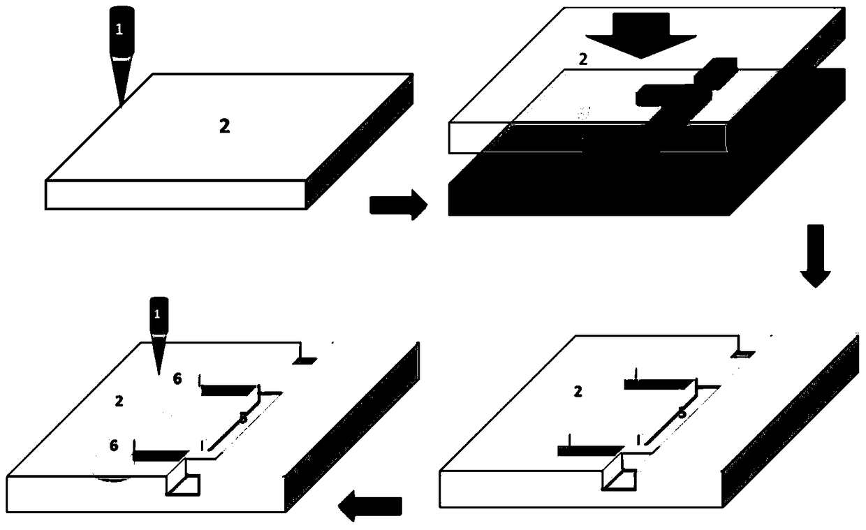
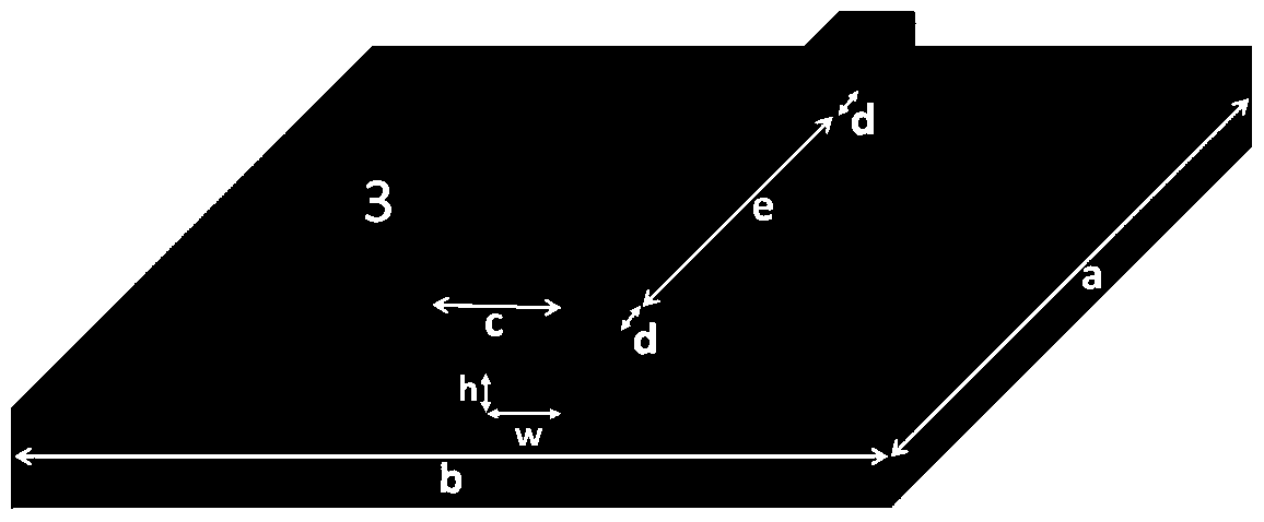
[0036] Use laser 1 to cut a surface-polished methyl methacrylate (PMMA) sheet with a thickness of 1mm (the glass transition temperature is 105°C), the cutting power is 50W, and the cutting speed is 10mm / s, and a rectangular microfluidic device is cut out. Substrate 2 (the length a is 4 cm, and the width b is 3 cm); then, a microfluidic channel groove is prepared by a thermal embossing method, and a silicon template 3 is used to emboss the groove by a thermal nanoimprint machine 4. The nanoimprint process Holding temperature 110°C, holding pressure 4kg / cm 2 , the holding time is 5 minutes, the template is naturally peeled off after imprinting, and the microfluidic channel groove 5 (line width 9 μm, depth 9 μm) is prepared. The length c of the leading and outgoing lines is 10 mm, and the length e of the middle line of the three-line structure is 20 mm. The two spacing...

Embodiment 2

[0042] Thermal nanoimprinting PMMA, core material SU-8-100

[0043] The specific process steps are as follows:

[0044] A surface-polished methyl methacrylate (PMMA) sheet with a thickness of 1mm (the glass transition temperature is 100°C) is cut with laser 1, the cutting power is 50W, and the cutting speed is 10mm / s, and a rectangular microfluidic tube is cut out. Thin sheet substrate 2 (4cm×2cm); Then prepare microfluidic channel grooves by hot embossing method, use polymer PDMS template, emboss grooves by thermal nanoimprint machine 4, the holding temperature of nanoimprint process is 120 ℃, holding pressure 1kg / cm 2 , the holding time is 10 minutes, the template is naturally peeled off after imprinting, and the microfluidic channel groove 5 (the line width is 40 μm, the depth is 40 μm) is prepared. 20mm, the two distances between the three line segments are both d is 40μm; the laser 1 is used to penetrate the ablation initial cylindrical liquid injection hole 6 at the po...

Embodiment 3

[0050] UV nanoimprint NOA63, core material SU-8-2005

[0051] The specific process steps are as follows:

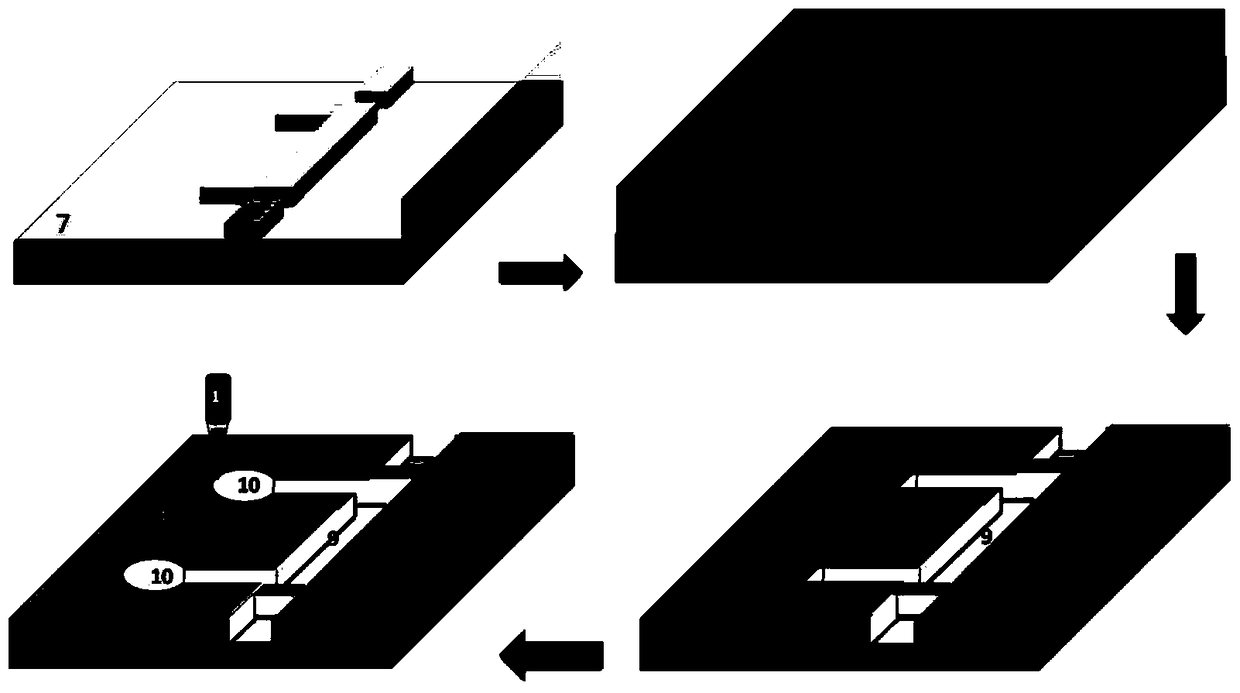
[0052] First, the liquid NOA63 material 7 is spin-coated on the surface of the polydimethylsiloxane PDMS imprint template 3 (there is a protruding three-segment structure on the template), the spin-coating rotation speed is 500r / min, and the spin-coating time is 20s to form a 0.5mm thick film, and then in a UV lamp (200mW / cm 2 ) fully exposed, exposed for 300s, solidified the liquid NOA63 material 7, and formed a solid NOA63 film 8, prepared a microfluidic channel groove 9 (the line width is 9 μm, and the depth is 9 μm) on the film, and the length c of the lead-in and lead-out lines is 10 mm. The length e of the middle line segment of the line segment structure is 20mm, and the distance between the two segments of the three line segments is 9 μm; a circular liquid injection hole 10 is ablated at the port of the groove with a laser 1 (the laser power is 40W, and the cutti...


PUM

PropertyMeasurementUnit
thicknessaaaaaaaaaa
lengthaaaaaaaaaa
widthaaaaaaaaaa

Abstract

The invention belongs to the polymer optical waveguide and micro fluidic channel integrated chip preparation technical field, and relates to a micro fluidic channel, mask, optical waveguide preparation and end face treatment method which concretely comprises: employing a nanoimprint (hot imprinting or ultraviolet imprinting) method to prepare micro fluidic grooves on a polymer substrate; a carbon dioxide laser cutting and penetrating injecting holes; evaporating an aluminum mask on a chip; spin coating photoresist; performing overall exposure and development to obtain a waveguide mask graph; utilizing a photosensitive polymer to prepare an optical waveguide core layer film on another substrate of the same material with a micro fluidic layer; performing hot imprinting packaging on two layers of chips; employing an upper layer micro fluidic chip as a photomask after packaging; writing in slab waveguide on a photosensitive polymer core layer film, wherein the waveguide is directly located under a micro fluidic channel, thereby avoiding register errors between the upper layer chip and a sensing window in an integration process; cutting a sample end face through laser, and completing an optical waveguide and micro fluidic registration-free integrated chip after polishing.

Description

technical field [0001] The invention belongs to the technical field of preparation of a three-dimensional hybrid integrated sensor chip of a polymer optical waveguide and a microfluidic channel, and specifically relates to a polymer photobleaching optical waveguide and a microfluidic plate-free integrated chip and a preparation method thereof. Background technique [0002] The optical waveguide liquid sensor chip uses the optical waveguide as the carrier of the optical signal, and realizes the sensing function by contacting the surface of the optical waveguide with the liquid to be tested. It has the characteristics of high sensitivity, fast response, simple structure, and anti-electromagnetic interference. , food safety, medical and health and other fields have a wide range of applications. According to the liquid introduction method, two methods are usually used: liquid storage tank and microfluidic channel. Microfluidic channel introduces liquid with controllable liquid f...

Claims


Application Information

Patent Timeline
Patent Type & Authority Patents(China)
IPC IPC(8): G02B6/12G02B6/13G03F7/00
CPCG02B6/12002G02B6/13G03F7/00
Inventor 衣云骥孙畅刘君实张大明王菲赵格格
Owner JILIN UNIV
Why Eureka
Try Eureka