Fin field-effect transistor formation method

A fin field effect transistor and fin technology, which is applied to semiconductor devices, electrical components, circuits, etc., can solve the problems of poor quality of stress layer and low electrical performance of fin field effect transistors, so as to achieve less etching damage and improve Electrical properties, highly selective effects

Active Publication Date: 2016-04-06
SEMICON MFG INT (SHANGHAI) CORP
View PDF5 Cites 7 Cited by
  • Summary
  • Abstract
  • Description
  • Claims
  • Application Information

AI Technical Summary

Problems solved by technology

[0007] However, the quality of the stress layer formed by the prior art is poor, resulting in poor electrical performance of the FinFET

Method used


Image

  • Fin field-effect transistor formation method
  • Fin field-effect transistor formation method
  • Fin field-effect transistor formation method

Examples


Embodiment Construction

[0037] It can be known from the background technology that the quality of the stress layer formed in the prior art is poor, which leads to poor performance of the fin-type field effect transistor.

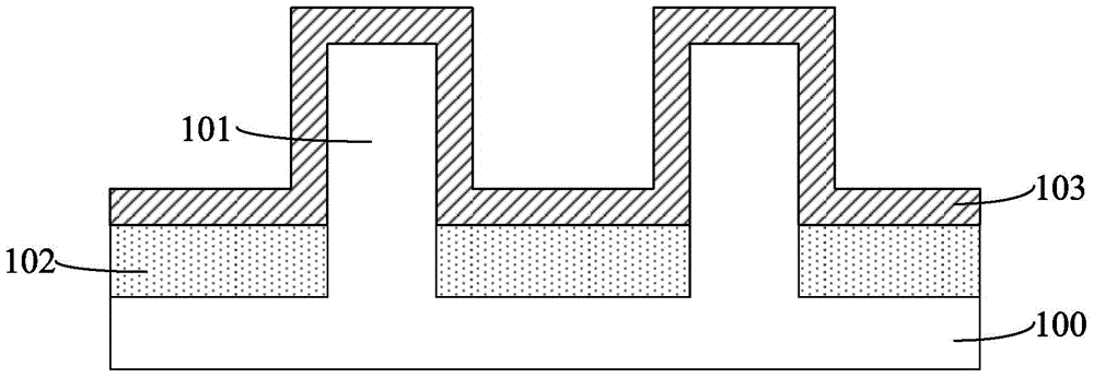
[0038] Please refer to figure 1 In one embodiment, a substrate 100 having fins 101 is provided, and an isolation layer 102 is formed on the surface of the substrate 100 between adjacent fins 101, and the isolation layer 102 covers part of the sidewall surface of the fin 101 , And the top surface of the isolation layer 102 is lower than the top surface of the fin 101; a barrier layer 103 covering the surface of the isolation layer 102, the sidewalls and the top surface of the fin 101 is formed.

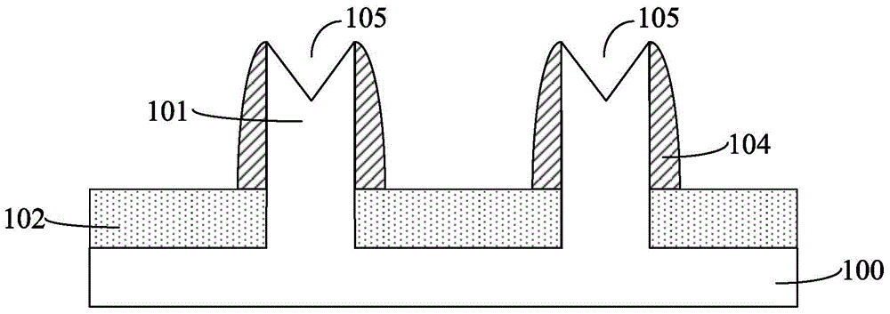
[0039] Please refer to figure 2 , Using a maskless etching process to etch and remove the barrier layer 103 located on the top surface of the fin 101 and the surface of the isolation layer 102 (please refer to figure 1 ), forming a sidewall layer 104 on the sidewall surface of the fin 101, exp...


PUM


Abstract

Provided is a fin field-effect transistor formation method which comprises the following steps: providing a substrate, and forming a plurality of independent fin portions on the surface of the substrate; forming an isolating layer on the surface of the substrate, the top surface of the isolating layer being lower than the top surface of each fin portion and the isolating layer covering a part of the surfaces of the side walls of the fin portions; forming a barrier layer covering the surface of the isolating layer and the top and side wall surfaces of the fin portions; converting a part of the barrier layer of a certain thickness into a passivation layer through oxidation treatment; etching back the passivation layer to form passivated side walls covering on the surface of the barrier layer on the side wall surfaces of the fin portions; and with the passivated side walls being as a mask, removing the barrier layer on the top surfaces of the fin portions by utilizing a wet etching process, and retaining the barrier layer on the side wall surfaces of the fin portions as barrier side walls. According to the fin field-effect transistor formation method, the quality of a formed stress layer is improved, and meanwhile, growth of the stress layer on the side wall surfaces of the fin portions can be prevented, and performance of a fin field-effect transistor is improved.

Description

Technical field [0001] The invention relates to the field of semiconductor manufacturing technology, in particular to a method for forming a fin-type field effect tube. Background technique [0002] With the continuous development of semiconductor process technology, the development trend of semiconductor process nodes following Moore's Law continues to decrease. In order to adapt to the reduction of process nodes, the channel length of the MOSFET has to be continuously shortened. The shortening of the channel length has the advantages of increasing the die density of the chip and increasing the switching speed of the MOSFET field effect tube. [0003] However, as the channel length of the device is shortened, the distance between the source and the drain of the device is also shortened. As a result, the gate's ability to control the channel becomes worse, and the gate voltage pinchoff the channel. The difficulty is getting bigger and bigger, making the phenomenon of subthreshold...

Claims


Application Information

Patent Timeline
Patent Type & Authority Applications(China)
IPC IPC(8): H01L21/336
CPCH01L29/7848H01L21/02326H01L21/02337H01L21/0234H01L29/66795H01L29/785H01L21/31111H01L21/31144H01L21/31116H01L29/165H01L21/0223H01L21/823468H01L21/02164H01L21/0217H01L21/0214H01L21/823431H01L27/0886
Inventor 禹国宾
Owner SEMICON MFG INT (SHANGHAI) CORP
Why Eureka
Try Eureka