Plasma processing apparatus

a processing apparatus and plasma technology, applied in the direction of coating, coating, chemical vapor deposition coating, etc., can solve the problems of difficult to achieve uniform etching and axial symmetry, unknown, and uneven etching rate, and achieve the effect of improving the uniformity of the surface of the wafer

Active Publication Date: 2011-12-13
HITACHI HIGH-TECH CORP
View PDF13 Cites 5 Cited by
  • Summary
  • Abstract
  • Description
  • Claims
  • Application Information

AI Technical Summary

Benefits of technology

[0011]Recently, integration of semiconductor devices has been improved and microfabrication, that is, machining accuracy has been required, while it has been more strictly required to improve uniformity of the etching rate or uniformity of a CD (Critical Dimension) in the machining dimensions on the wafer.
[0016]In order to overcome the above problems, the invention provides a plasma processing apparatus that is suitable for microfabrication by improving uniformity of the surface of a wafer shaped for etching.
[0018]To achieve the above configuration, the invention provides a plasma processing apparatus that is suitable for microfabrication by improving uniformity of the surface of a wafer shaped for etching.

Problems solved by technology

Further, the effect of improving the uniformity of the etching rate or the axial symmetry achieved by rotating the microwave electric field or making the gas flow uniform has not been apparently known.
In this method, because the factors that influence the uniformity of etching, etc. are different for each step, it is difficult to achieve uniformity of etching and axial symmetry when etching of each multi-layer is finished.

Method used


Image

  • Plasma processing apparatus
  • Plasma processing apparatus
  • Plasma processing apparatus

Examples


first embodiment

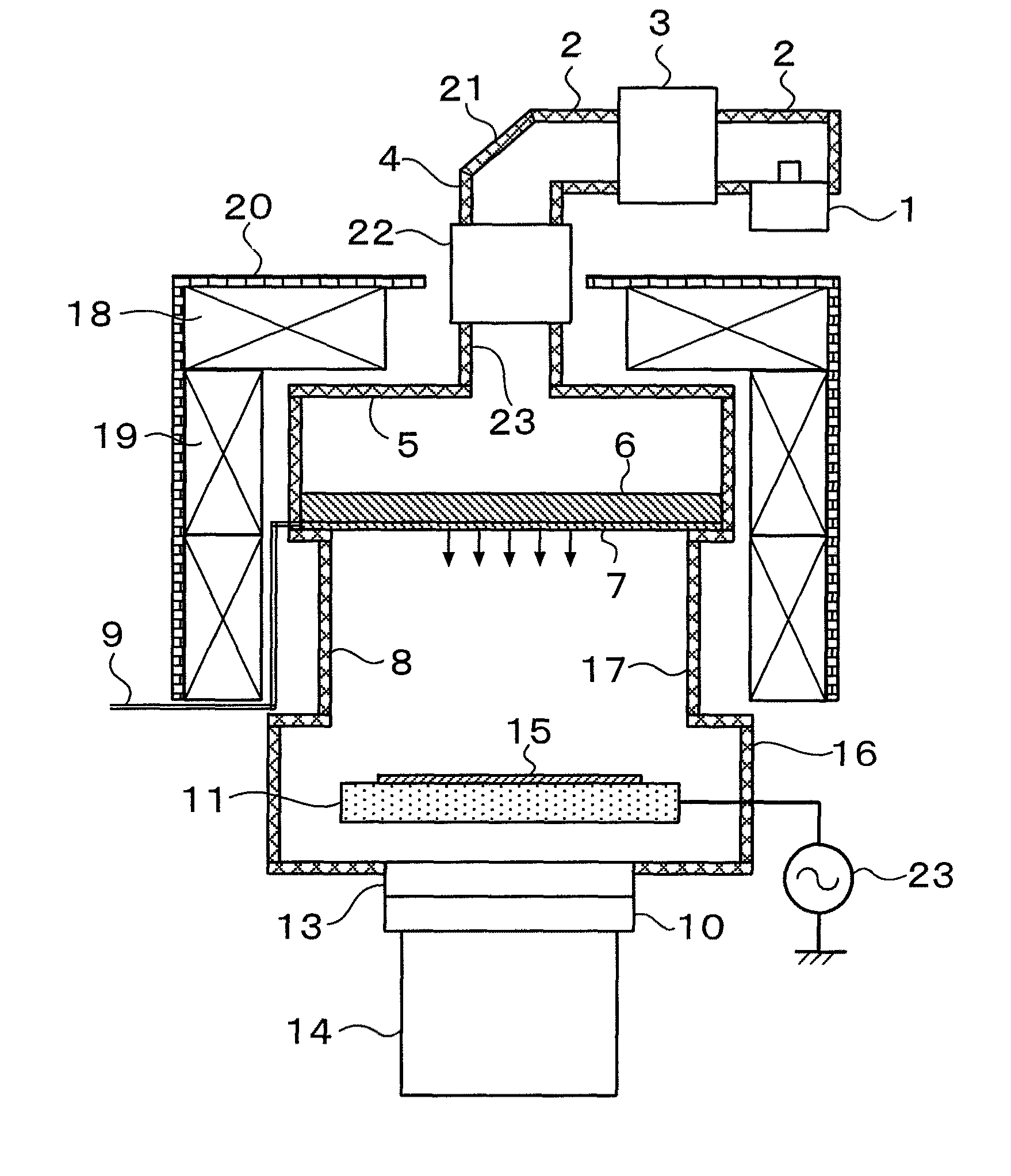
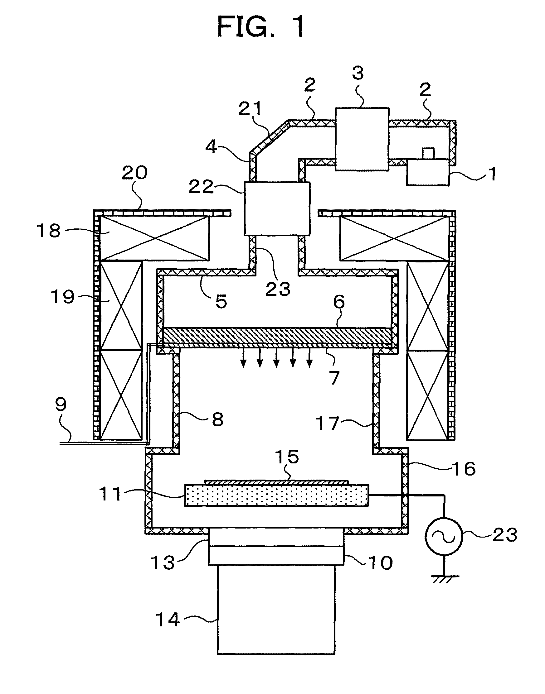
[0029]Preferred embodiments of the invention are described hereafter with reference to the accompanying drawings. FIG. 1 is a view illustrating a plasma processing apparatus (an apparatus equipped with a cavity resonator for dry-etching of a microwave having a magnetic field) according to the invention. As shown in FIG. 1, a decompression chamber 8 is provided with a vacuum container 16, a discharge tube 17, and a quartz plate 6. The pressure inside the chamber 8 is decreased by actuating a vacuuming device 14 with an on-off exhaust valve 13 open.

[0030]Process gas such as etching gas, passes through a mass flow controller (not shown), a gas pipe 9, and a gap between the quartz plate 6 and a quartz shower plate 7, and then flows into the chamber 8 through gas holes of the quartz shower plate 7. The etching gas that has flowed in the chamber 8 is discharged through an exhaust speed-varying valve 10 adjusting the exhaust speed by the vacuuming device 14, such that the inside pressure o...

second embodiment

[0062]FIG. 7 is a view illustrating an apparatus equipped with a cavity resonator for dry-etching of a microwave having a magnetic field according to a In this example, separate coolant grooves 30a, 30b are formed on the inside and the outside of the wafer-placing electrode 11 as shown in FIG. 7, coolant is provided to the coolant grooves through separate chiller unit. Accordingly, it is possible to control temperature distribution over the surface of the wafer 15. In this embodiment, the electrode including the coolant grooves 30 is formed such that the temperature distribution of the wafer 15 is axially symmetric.

[0063]With the axially-symmetric gas flow and the electric field distribution of a microwave on the wafer 15, the etching characteristics including the CD value can be axially symmetrically distributed. Further, supposing that the temperature of the wafer is axially symmetrically distributed, radial direction temperature distribution of the wafer can be controlled. In th...

third embodiment

[0064]FIG. 8 is a view illustrating an apparatus equipped with a cavity resonator for dry-etching of a microwave having a magnetic field according to a In this embodiment, heaters 31a, 31b are embedded in the inside and outside of the wafer-placing electrode 11 such that the temperature of the wafer 15 is axially symmetrically distributed and the heaters are connected to heater power supplies (not shown). Further, a coolant groove (not shown) is formed on the wafer-placing electrode 11 and a chiller unit (not shown) is connected to the coolant groove. Therefore, it is possible to improve time response to the temperature of the wafer.

[0065]In etching a multi-layer, etching conditions should be sequentially changed for each layer of the multi-layer; however, it is possible in this embodiment to optimize the temperature distribution or the absolute temperature of the wafer 15 at each etching step, easily improve the uniformity of the surface of the wafer 15 in the etching characterist...


PUM

PropertyMeasurementUnit
frequencyaaaaaaaaaa
magnetic flux densityaaaaaaaaaa
magnetic fieldaaaaaaaaaa

Abstract

A plasma processing apparatus includes: a decompression chamber of which the inside is depressed; a gas supply unit that supplies process gas into said chamber; a microwave supply unit that supplies a microwave into the chamber to generate plasma; an object-placing electrode where a processing material, is placed and which holds the processing material in the chamber; and a vacuuming unit that is connected to the chamber to discharge the gas in the chamber, in which the chamber, a part for providing gas into the chamber of the gas supply unit, a part for introducing a microwave into the chamber of the microwave supply unit, the object-placing electrode, and the vacuuming unit are disposed coaxially with the center axis of the chamber, and the part for introducing a microwave includes a microwave rotation generator that rotates a polarization plane of the input microwave and supplies the microwave to the chamber.

Description

BACKGROUND OF THE INVENTION[0001]1. Field of the Invention[0002]The present invention relates to a plasma processing apparatus, particularly a plasma processing apparatus that can improve the uniformity of a processing surface of a wafer.[0003]2. Description of the Related Art[0004]A microwave plasma processing apparatus having a magnetic field for etching, for example, introduces a microwave into a decompression chamber through a wave guide and a cavity resonator, generates plasma in the chamber using interaction of the introduced microwave with a magnetic field produced by a magnetic field-producing coil, and etches processing objects, such as a wafer.[0005]In general, the frequency of a microwave is 2.45 GHz and the microwave travels, in a circular TE11 mode, through the wave guide and is introduced into the chamber. The electric field of the microwave of the circular TE11 mode is distributed in an elliptical shape, as disclosed in ‘Microwave Engineering’ by Nakajima Masamitsu, p...

Claims


Application Information

Patent Timeline
Patent Type & Authority Patents(United States)
IPC IPC(8): C23C16/00C23F1/00H01L21/306
CPCH01J37/32192H01J37/32229H01J37/32293H01J37/32449H01J2237/2001
Inventor WATANABE, SEIICHIYASUI, NAOKITAUCHI, SUSUMUNISHIMORI, YASUHIRO
Owner HITACHI HIGH-TECH CORP
Why Eureka
Try Eureka