Method of etching object to be processed

a processing method and object technology, applied in the field of etching objects, can solve the problems of uneven etching rate on the surface of a wafer in the processing container, deterioration of the quality of the wafer after etching, etc., and achieve the effect of improving the uniformity of etching ra

Active Publication Date: 2018-11-22
TOKYO ELECTRON LTD
View PDF3 Cites 4 Cited by
  • Summary
  • Abstract
  • Description
  • Claims
  • Application Information

AI Technical Summary

Benefits of technology

[0013]As described above, during plasma etching, the uniformity of the etching rate is improved.

Problems solved by technology

However, in the plasma etching as disclosed in, for example, Patent Document 1, deviation occurs in the distribution of the density of plasma in a processing container according to the configuration of a plasma processing apparatus (e.g., the shape of the processing container), and by this deviation, the etching rate on the surface of a wafer in the processing container becomes uneven.
When the etching rate is uneven, the quality of the wafer after etching deteriorates, which is also undesirable from the viewpoint of manufacturing efficiency.

Method used


Image

  • Method of etching object to be processed
  • Method of etching object to be processed
  • Method of etching object to be processed

Examples


modification 1

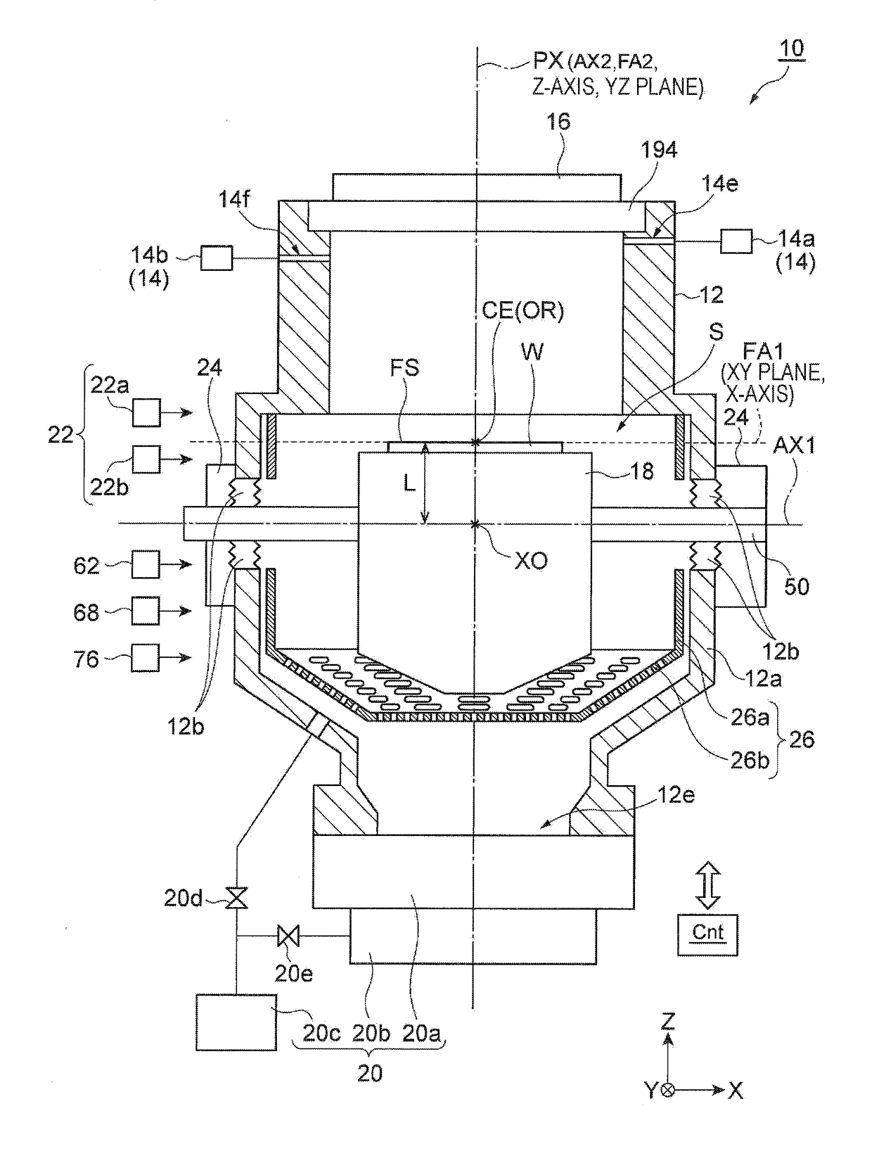
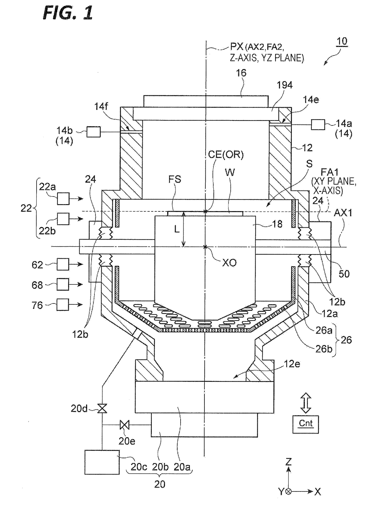
[0176]For example, when considering a case of moving the inclination shaft unit 50 (the first axis AX1) along the axis PX (in other words, a case of moving the position of the intersection point XO of the second axis AX2 (the central axis of the wafer W) and the axis PX (the reference axis of the processing container 12) along the axis PX), the predicted distribution of the etching rate [μm / min] such as, for example, PER1(x, y, z; φ; CON) differs according to the combination of the value φ [Deg.] of the inclination angle AN, the etching condition CON of the etching performed in the processing container 12, and the position on the axis PX of the intersection point XO of the first axis AX1 and the axis PX (specifically, for example, the distance L between the intersection point XO and the horizontal reference plane FA1). In this case, the respective values of the parameters α, β, γ, ζ, and ξ are determined for each state in a case of obtaining actually measured values used for specify...

modification 2

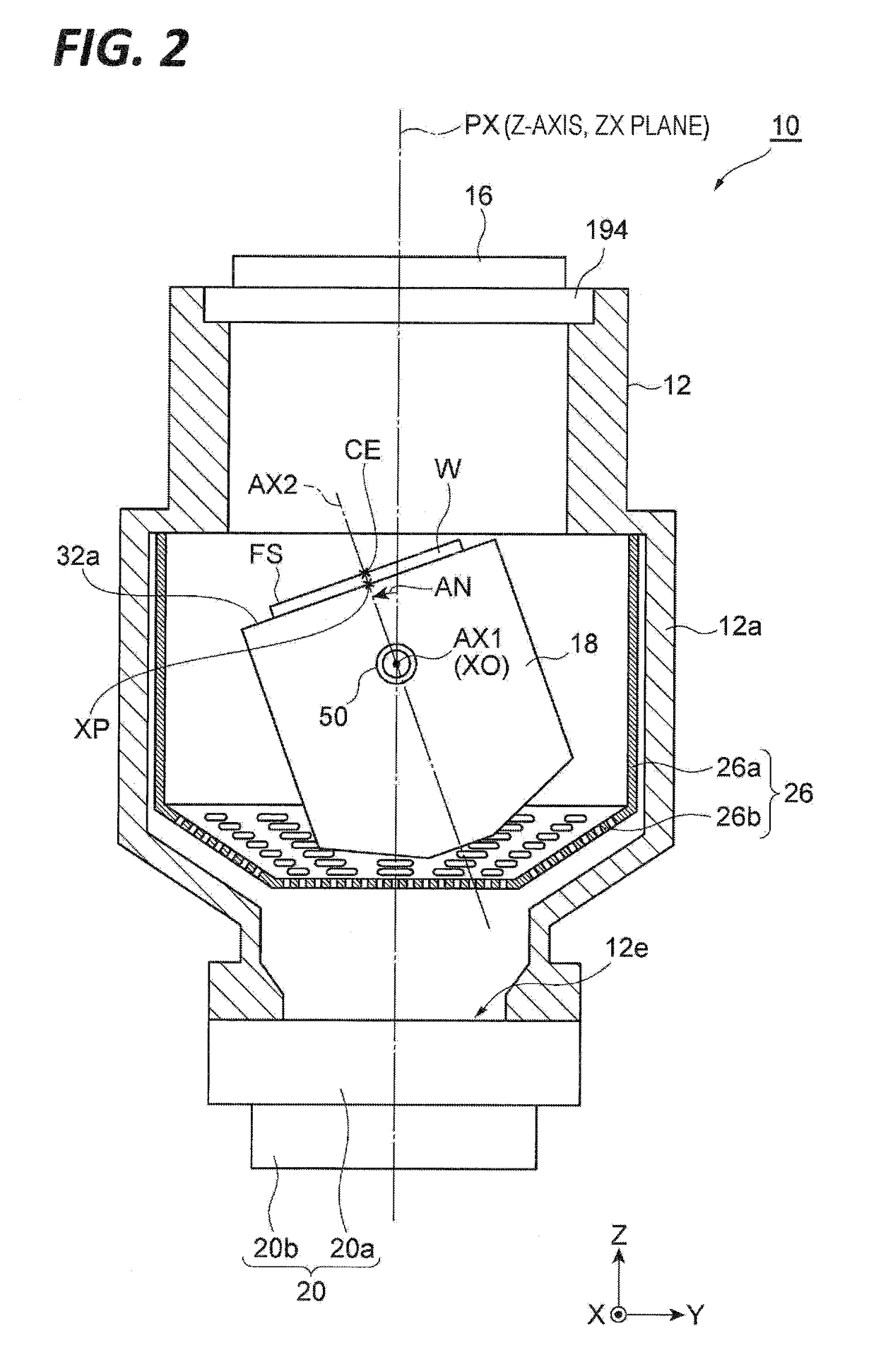
[0180]The holding structure 18 may have a configuration in which the electrostatic chuck 32, the lower electrode 34, and the rotary shaft unit 36 are movable along the second axis AX2. In this configuration, when considering a case of moving the upper surface 32a (the surface holding the wafer W) of the electrostatic chuck 32 along the second axis AX2 (the central axis of the wafer W) (in other words, a case of moving the position of the intersection point XP of the upper surface 32a of the electrostatic chuck 32 and the second axis AX2 along the second axis AX2 while maintaining the orientation of the upper surface 32a), the predicted distribution of the etching rate such as PER1(x, y, z; φ; CON) differs according to the combination of the value φ [Deg.] of the inclination angle AN, the etching condition CON of etching performed in the processing container 12, and the position on the second axis AX2 of the intersection point XP of the upper surface 32a of the electrostatic chuck 32...


PUM

PropertyMeasurementUnit
voltageaaaaaaaaaa
frequencyaaaaaaaaaa
frequencyaaaaaaaaaa

Abstract

A method MT includes etching a wafer W using plasma generated in a processing container. The etching includes a process of inclining and rotating a holding structure holding the wafer W during execution of the etching and the process successively creating a plurality of inclined rotation states RT(φ, t) with respect to the holding structure. In the inclined rotation states, the wafer W is rotated about a central axis of the wafer W over a predetermined process time while maintaining a state where the central axis is inclined with respect to a reference axis of the processing container which is in the same plane as the central axis. A combination of a value φ of an inclination angle AN of the central axis with respect to the reference axis and the process time t differs for each of the plurality of inclined rotation states.

Description

TECHNICAL FIELD[0001]Exemplary embodiments of the present disclosure relate to a method of etching an object to be processed (“workpiece”).BACKGROUND[0002]As a type of memory element using a magnetoresistive effect element, a magnetic random access memory (MRAM) element having a magnetic tunnel junction (MTJ) structure has attracted attention. The MRAM element includes a multilayer film formed of a hard-to-etch material containing a metal such as, for example, a ferromagnetic material. In a step of manufacturing such an MRAM element, the multilayer film is etched using a mask formed of a metal material such as, for example, tantalum (Ta) or TiN.[0003]In such etching, a halogen gas has been used in the art as described in Patent Document 1. The manufacturing method disclosed in Patent Document 1 is a method of manufacturing a semiconductor device, which includes a step of forming a magnetoresistive effect element using a magnetic material including at least one of cobalt, iron, and n...

Claims


Application Information

Patent Timeline
Patent Type & Authority Applications(United States)
IPC IPC(8): H01J37/32C23F4/00H01L43/12H01F41/34H01F10/32
CPCH01J37/32715C23F4/00H01L43/12H01F41/34H01F10/3254H01J2237/3343H01J2237/20214H01J2237/20207G11C11/161H01L43/02H01L43/10H01J37/3211H01J2237/002H01F41/308H10N50/01H01L21/3065H01L21/683H01L27/105H05H1/46H10N50/10H10N50/80H10N50/85
Inventor UMEZAWA, YOSHIHIROSATO, JUNMAEDA, KIYOSHIOHATA, MITSUNORIMATSUMOTO, KAZUYA
Owner TOKYO ELECTRON LTD
Why Eureka
Try Eureka