LED supersonic packaging method
A packaging method and ultrasonic technology, applied in non-electric welding equipment, electrical components, circuits, etc., can solve the problems of large internal stress, easy aging, poor heat resistance, etc., to improve welding efficiency, ensure welding quality, and shorten welding time. Effect
- Summary
- Abstract
- Description
- Claims
- Application Information
AI Technical Summary
Problems solved by technology
Method used
Image
Examples
Embodiment 1
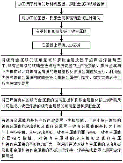
[0028] In this example, see Figure 1~5 , an LED ultrasonic packaging method, the steps are as follows:
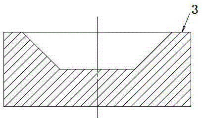
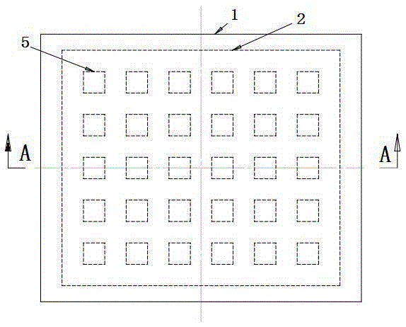
[0029] a. Process the raw material substrate 3, expanded metal plate 2, and glass cover plate 1 for packaging. The expanded metal plate 2 is provided with a hollow LED light-emitting window 5. The light-emitting window 5 is a gap processed according to the packaging structure and size of the LED chip 4. , the glass cover plate 1 is made of quartz glass or borosilicate glass, the expanded metal plate 2 is made of Kovar alloy, the substrate 3 is made of ceramic substrate or aluminum substrate, and the substrate 3 has a groove for welding the LED chip 4, and the processed substrate 3 The peripheral dimension is 5×5×2mm, the peripheral dimension of the processed expanded metal plate 2 is 52×44×0.2mm, and the size of each notch for cutting the light-emitting window 5 inside the processed expanded metal plate 2 is 4×4×0.2mm , the number of rows and columns of the array of ligh...
Embodiment 2
[0038] This embodiment is basically the same as Embodiment 1, especially in that:
[0039] In this example, see Figure 6-8 , an LED ultrasonic packaging method, the steps are as follows:
[0040] a. Process the raw material substrate 3, expanded metal plate 2, and glass cover plate 1 for packaging. The expanded metal plate 2 is provided with a hollow LED light-emitting window 5. The light-emitting window 5 is a gap processed according to the packaging structure and size of the LED chip 4. , the glass cover plate 1 is made of quartz glass or borosilicate glass, the expanded metal plate 2 is made of Kovar alloy, the substrate 3 is made of ceramic substrate or aluminum substrate, and the substrate 3 has a groove for welding the LED chip 4, and the processed substrate 3 The peripheral dimension is 5×5×2mm, the peripheral dimension of the processed expanded metal plate 2 is 55.5×46.5×0.4mm, and the upper stepped surface of each upper step-shaped notch part of the cutout is proce...
PUM
 Abstract
Description
Claims
Application Information
 - R&D Engineer
- R&D Manager
- IP Professional
- Industry Leading Data Capabilities
- Powerful AI technology
- Patent DNA Extraction
Browse by: Latest US Patents, China's latest patents, Technical Efficacy Thesaurus, Application Domain, Technology Topic, Popular Technical Reports.
© 2024 PatSnap. All rights reserved.Legal|Privacy policy|Modern Slavery Act Transparency Statement|Sitemap|About US| Contact US: help@patsnap.com


