


Quick Research
Generate reliable direction feasibility study reports for your R&D in just a few steps.

Technical Q&A
Discover and master advanced knowledge NOW. Basics, ideas, possibilities, all at once.

Find Solutions
As an expert in R&D theories, this can generate solutions to your technical problems instantly.

Evaluate Feasibility
Analyze your overall solution with one click, know your potential R&D risks in advance.

Monitor Landscape
Get weekly tech updates, stay abreast of the latest tech innovations and key insights.
A method to reduce the ohmic contact resistance of gan HEMT devices
A technology of ohmic contact and resistance, which is applied in semiconductor devices, semiconductor/solid-state device manufacturing, circuits, etc. It can solve the problems of difficult reduction of resistivity and ohmic contact resistance, so as to reduce ohmic contact resistance, reduce alloy temperature, and improve devices Effect of Contact Resistivity
- Summary
- Abstract
- Description
- Claims
- Application Information
AI Technical Summary
Problems solved by technology
Method used
Image

Examples
preparation example Construction
[0023] (2) Preparation of composite medium layer;
[0024] (3) Fabrication of Ni nanomask in ohmic region;
[0025] (4) Ni nanomask / SiO 2 Fabrication of nanopillars;
[0026] (5) Transfer of nanopillar pattern to Si 3 N 4 on the mask;
[0027] (6) The formation of micropores in the barrier layer and channel layer region;
[0028] (7) Evaporation / stripping / annealing to form ohmic contacts.
[0029] Attached below Figure 2-1~Figure 2-9 , further describe the technical scheme of the present invention:
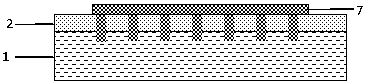
[0030] (1) On the GaN heterojunction material formed by AlGaN barrier layer 2 / GaN channel layer 1, 100 nmSi was grown by PECVD 3 N 4 3 and 100nm SiO 2 4 Composite dielectric layers, such as diagram 2-1 shown;
[0031] (2) Coat a layer of AZ7908 photoresist on the sample by spinning glue and pre-baking, and define the source and drain regions through photolithography exposure, development and post-baking processes, and use electron beam evaporation equipment to evap...
Embodiment 1
[0040] Reducing the ohmic contact resistance of GaN HEMT devices based on nano-micropore technology includes the following steps:
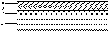
[0041] (1) The channel layer 1 of a GaN heterojunction material with a two-dimensional electron gas is GaN, AlGaN or InGaN material, and the barrier layer 2 is grown on a material containing AlGaN, InAlN or AlN 3 N 4 3 and SiO 2 4 composite dielectric layers; the Si 3 N 4 3 and SiO 2 4 Dielectric materials can be grown by PECVD, sputtering and thermal evaporation, among which Si 3 N 4 3 and SiO 2 4 The thickness of the medium is 50nm, Si 3 N 4 3 The etching rate of materials in buffered hydrofluoric acid solution is higher than that of SiO 2 4 The material should be more than 5 times lower;
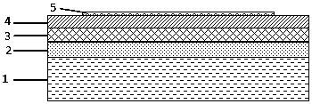
[0042] (2) Use photolithography to define the ohmic region, evaporate a thin layer of Ni metal 5 in the ohmic contact region, and use the metal lift-off process to peel off the thin Ni metal 5 in the ohmic region; the thickness of the thin N...
Embodiment 2
[0050] Reducing the ohmic contact resistance of GaN HEMT devices based on nano-micropore technology includes the following steps:
[0051] (1) The channel layer 1 of a GaN heterojunction material with a two-dimensional electron gas is GaN, AlGaN or InGaN material, and the barrier layer 2 is grown on a material containing AlGaN, InAlN or AlN 3 N 4 3 and SiO 2 4 composite dielectric layers; the Si 3 N 4 3 and SiO 2 4 Dielectric materials can be grown by PECVD, sputtering and thermal evaporation, among which Si 3 N 4 3 and SiO 2 4 The thickness of the medium is between 50nm and 200nm, Si 3 N 4 3 The etching rate of materials in buffered hydrofluoric acid solution is higher than that of SiO 2 4 The material is more than 6 times lower;
[0052] (2) Use photolithography to define the ohmic region, evaporate a thin layer of Ni metal 5 in the ohmic contact region, and use the metal lift-off process to peel off the thin Ni metal 5 in the ohmic region; the thickness of...
PUM
| Property | Measurement | Unit |
|---|---|---|
| thickness | aaaaa | aaaaa |
| thickness | aaaaa | aaaaa |
| thickness | aaaaa | aaaaa |
Abstract
Description
Claims
Application Information
 - R&D Engineer
- R&D Manager
- IP Professional
- Industry Leading Data Capabilities
- Powerful AI technology
- Patent DNA Extraction
Browse by: Latest US Patents, China's latest patents, Technical Efficacy Thesaurus, Application Domain, Technology Topic, Popular Technical Reports.
© 2024 PatSnap. All rights reserved.Legal|Privacy policy|Modern Slavery Act Transparency Statement|Sitemap|About US| Contact US: help@patsnap.com