Low-damage indium gallium arsenic detector p+n junction preparation method
An indium gallium arsenic and detector technology, applied in the field of infrared detector preparation, can solve the problems of reducing surface state density, reducing recombination centers, and large junction damage, etc., achieving a good process foundation, suppressing the generation of dark current, and suppressing dark current Effect
- Summary
- Abstract
- Description
- Claims
- Application Information
AI Technical Summary
Problems solved by technology
Method used
Image
Examples
Embodiment 1
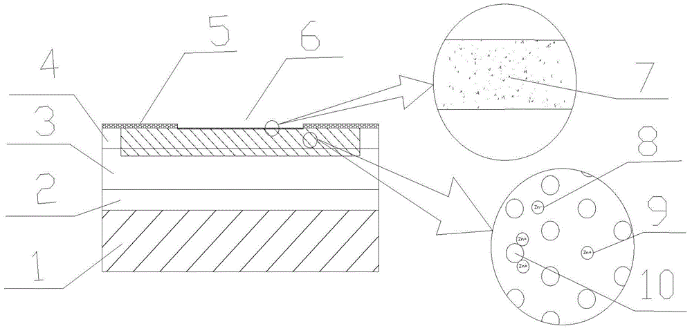
[0037] 1. Deposit silicon nitride diffusion mask 5, using plasma enhanced chemical vapor deposition (PECVD) technology to deposit silicon nitride junction mask 5 with a thickness of 200±30nm, the substrate temperature is 330±20°C, RF The power is 40±10W;
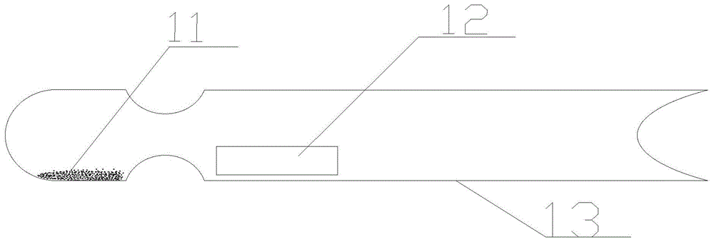
[0038] 2. First use the inductively coupled plasma (ICP) etching technology to open the window 6, and then put the element ion source 11 and the epitaxial wafer 12 into the source area and the sample area of the quartz chamber 13 in sequence, such as figure 1 As shown, evacuate to 3×10 -4 Below Pa, then seal the quartz chamber 13, keep it at a temperature of 550±20°C for 9±3min, and then take it out quickly;
[0039] 3. Sampling and cleaning, opening the quartz chamber 13, taking out the epitaxial wafer 12, cleaning with chloroform, ether, acetone, and MOS grade ethanol, and drying with high-purity nitrogen.
[0040] 4. Heat treatment in a nitrogen atmosphere, put sample 12 into a thermal annealing furnace, maintain a n...
Embodiment 2
[0043] 1. Deposit silicon nitride diffusion mask 5, using plasma enhanced chemical vapor deposition (PECVD) technology to deposit silicon nitride junction mask 5 with a thickness of 200±30nm, the substrate temperature is 330±20°C, RF The power is 40±10W;
[0044] 2. First use the inductively coupled plasma (ICP) etching technology to open the window 6, and then put the element ion source 11 and the epitaxial wafer 12 into the source area and the sample area of the quartz chamber 13 in sequence, such as figure 1 As shown, evacuate to 3×10 -4 Below Pa, then seal the quartz chamber 13, keep it at a temperature of 550±20°C for 9±3min, and then take it out quickly;
[0045] 3. Sampling and cleaning, opening the quartz chamber 13, taking out the epitaxial wafer 12, cleaning with chloroform, ether, acetone, and MOS grade ethanol, and drying with high-purity nitrogen.
[0046] 4. Heat treatment in a nitrogen atmosphere, put sample 12 into a thermal annealing furnace, maintain a n...
Embodiment 3
[0049] 1. Deposit silicon nitride diffusion mask 5, using plasma enhanced chemical vapor deposition (PECVD) technology to deposit silicon nitride junction mask 5 with a thickness of 200±30nm, the substrate temperature is 330±20°C, RF The power is 40±10W;
[0050] 2. First adopt the inductively coupled plasma (ICP) etching technology to open the window 6, and then put the element ion source 11 and the epitaxial wafer 12 into the source area and the sample area of the quartz chamber 13 in sequence, such as figure 1 As shown, evacuate to 3×10 -4Below Pa, then seal the quartz chamber 13, keep it at a temperature of 550±20°C for 9±3min, and then take it out quickly;
[0051] 3. Sampling and cleaning, opening the quartz chamber 13, taking out the epitaxial wafer 12, cleaning with chloroform, ether, acetone, and MOS grade ethanol, and drying with high-purity nitrogen.
[0052] 4. Heat treatment in a nitrogen atmosphere. Put sample 12 into a thermal annealing furnace and maintain...
PUM
 Abstract
Description
Claims
Application Information
 - R&D Engineer
- R&D Manager
- IP Professional
- Industry Leading Data Capabilities
- Powerful AI technology
- Patent DNA Extraction
Browse by: Latest US Patents, China's latest patents, Technical Efficacy Thesaurus, Application Domain, Technology Topic, Popular Technical Reports.
© 2024 PatSnap. All rights reserved.Legal|Privacy policy|Modern Slavery Act Transparency Statement|Sitemap|About US| Contact US: help@patsnap.com


