
Double-end assembly line type copy bit line circuit

A kind of duplicating bit line and pipeline type technology, applied in the direction of information storage, static memory, digital memory information, etc., can solve the problems of SRAM chip performance degradation, affecting chip speed, increasing bit line precharge time, etc.

Active Publication Date: 2015-04-29
ANHUI UNIVERSITY
View PDF6 Cites 0 Cited by
  • Summary
  • Abstract
  • Description
  • Claims
  • Application Information

AI Technical Summary

Problems solved by technology

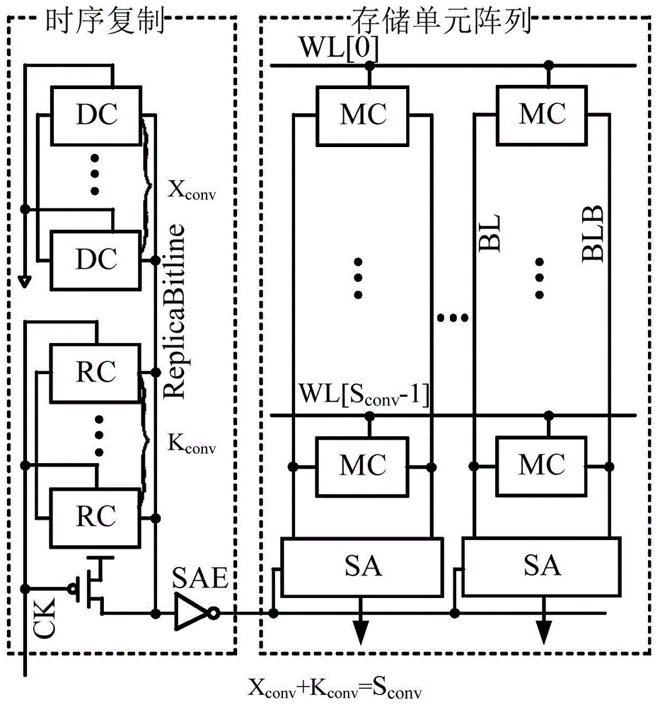
However, with the progress of the process, this traditional bit line replication technology can no longer improve the timing deviation problem, especially when the power supply voltage is reduced, the process deviation will become very poor, so that the performance of the SRAM chip will be greatly reduced
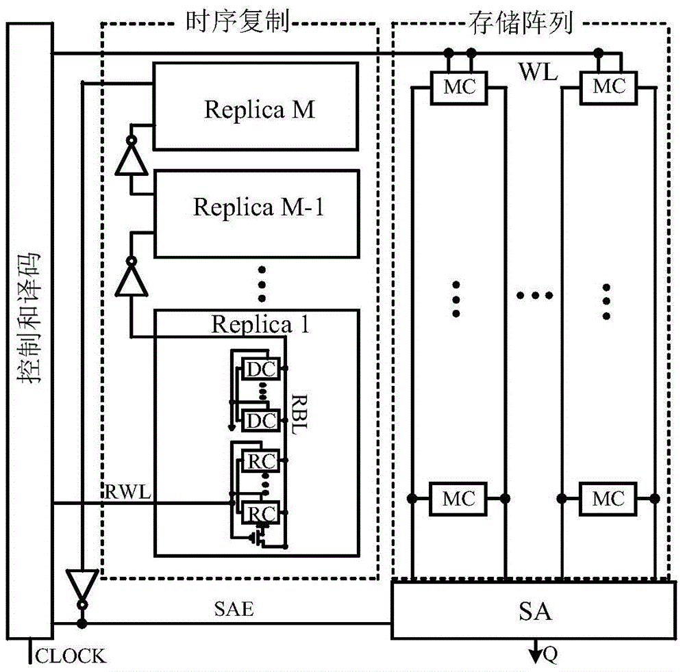
[0005] (2) if figure 2 The timing replication module shown in is a multi-level replication bit line technology circuit structure, which divides the bit line into M stages on the basis of the traditional replication bit line, and connects each stage in series through an inverter. The last stage of inverter outputs SAE, in which the replica unit RC of each replica bit line is equal and consistent with the number of traditional replica cells RC, therefore, the discharge delay time and discharge timing process deviation of each replica bit line are the traditional discharge Delay time and 1 / M of process deviation. According to statistical principles, the total discharge delay after superimposition of divided M-level replica bit lines is equal to the discharge delay of traditional replica bit line circuits, but the total process deviation after superposition is only for traditional replicating bitlines But with the increase of M, the gate delay and quantization error brought by the inverter will not be negligible
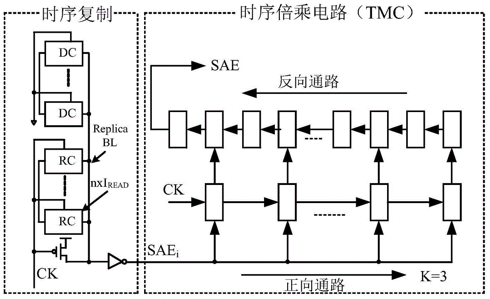
[0006] (3) if image 3 The circuit structure shown is a digital copy bit line technology, which is composed of a timing copy module and a timing multiplication circuit; this technology increases the number of copying units RC for copying bit lines in the timing copying module to K times that of the traditional copying unit RC, According to statistical principles and related conclusions, the discharge delay time and process deviation of the timing replication module are respectively 1 / K and 1 / K of the traditional replication bit line. Therefore, on the basis of ensuring that the discharge delay time of the traditional replicated bit line is equal, the digital replicated bit line circuit needs to introduce a timing multiplication circuit TMC in addition to the timing replication module. By multiplying the timing by K times, the final timing deviation are conventionally replicated bit lines of the However, since the timing multiplication circuit introduced is composed of a large number of delay units, this will cause a large waste of chip area
At the same time, the quantization error and process deviation of these delay units cannot be ignored. At low voltage, the deviation of the multiplier circuit deteriorates more seriously, and even exceeds the process deviation of the copied bit line.
[0007] (4) if Figure 4 Shown is a multi-level parallel copy bit line technology circuit structure, the circuit divides the copy bit line into M stages, and at the same time increases the number of copy units RC by K times, using the digital delay unit DDC in the timing accumulation circuit (TAC) The discharge time of each level of replication unit is copied in parallel, and finally the final SAE is superimposed and output through the M*K level digital delay unit DDC, so the process deviation is reduced to that of the traditional replication bit line The essence of this technology is to copy K bit lines, and the M*K digital delay unit DDC circuit in the timing accumulation circuit TAC is also composed of a large number of delay units, which greatly increases the area of ​​the chip, especially when M increases, it will waste more chip area
[0008] (5) if Figure 5 The timing replication module shown in is a dual-replication bit-line technology circuit structure, which makes full use of the two bit lines of the traditional replication bit line, and combines the two bit lines, using a new double-ended replication unit RC , on the basis of keeping the circuit area of ​​the traditional replicated bit line unchanged, the process deviation can be reduced to that of the traditional replicated bit line However, due to the larger capacitance of the bit line, this will increase the pre-charge time of the bit line, which will lead to an increase in the overall access time of the SRAM and affect the chip speed.

Method used


Image

  • Double-end assembly line type copy bit line circuit
  • Double-end assembly line type copy bit line circuit
  • Double-end assembly line type copy bit line circuit

Examples


Embodiment 1

[0059] Image 6 It is a schematic structural diagram of a double-ended pipeline replication bit line circuit provided by Embodiment 1 of the present invention. like Image 6 As shown, the circuit mainly includes:

[0060] The first inverter INV1, the second inverter INV2, the third inverter INV3, the first NAND gate NAND1, the first replica bit line RBL, the second replica bit line RBLB, the first pre-filled PMOS transistor PR1, The second pre-charged PMOS transistor PR2, the first D flip-flop DFF 1 to the Nth D flip-flop DFF N , the first control circuit CTL 1 to the Nth control circuit CTL N , the first charging PMOS transistor P 1 To charge the Nth PMOS transistor P N , N / 2 sets of replication units RC and a set of X redundancy units DC in total of K in each group; wherein, N is an even number, indicating the number of times of flow;

[0061] The PR signal is connected to the gates of the first pre-charged PMOS transistor PR1 and the second pre-charged PMOS transist...

Embodiment 2

[0083] Figure 7 A schematic structural diagram of yet another double-ended pipeline replication bit line circuit provided by Embodiment 2 of the present invention. like Figure 7 As shown, it mainly includes:

[0084] The first inverter INV1, the second inverter INV2, the third inverter INV3, the first NAND gate NAND1, the first replica bit line RBL, the second replica bit line RBLB, the first pre-filled PMOS transistor PR1, The second pre-charged PMOS transistor PR2, the first D flip-flop DFF 1 to the Nth D flip-flop DFF N , the first control circuit CTL 1 to the Nth control circuit CTL N , the first charging PMOS transistor P 1 To charge the Nth PMOS transistor P N , each group of K total (N+1) / 2 groups of replication units RC and a group of X redundancy units DC; wherein, N is an odd number, indicating the number of times of flow;

[0085] The PR signal is connected to the gates of the first pre-charged PMOS transistor PR1 and the second pre-charged PMOS transistor...


PUM


Abstract

The invention discloses a double-end assembly line type copy bit line circuit. According to the circuit, two implementation modes are realized according to different assembly line frequencies, the process deviation of a sense amplifier control timing sequence generation circuit in SRAM can be reduced by the circuit, the process tolerance of the sense amplifier control timing sequence generation circuit in the SRAM is improved, the process deviation can be reduced into 1 / [k*(arithmetic square root of M)] of the traditional copy bit line under the conditions that the bit line pre-charging time is not influenced and the design area is not greatly increased, and in order to guarantee that the average delay of the circuit is equal to that of the traditional copy bit line circuit, the assembly line frequency N is equal to M*K. Moreover, when M is equal to 1, namely when the copy bit line length is equal to the traditional length, the obtained process deviation of SAE is minimum and is equal to 1 / N of the deviation of SAE generated by the traditional copy bit line.

Description

technical field [0001] The invention relates to the field of integrated circuit (IC) design, in particular to a double-end pipeline type copy bit line circuit. Background technique [0002] With the development of technology level, higher speed, lower power consumption and smaller area pursued by integrated circuit design have become the main design direction. As a basic IP core, SRAM plays an indispensable role in integrated circuit design. The main way to reduce power consumption at this stage is to reduce the power supply voltage, that is, the power consumption is linearly related to the square of the power supply voltage. Therefore, by reducing the power supply voltage, the Significantly reduce power consumption; however, as the power supply voltage drops, the process deviation of the designed circuit will increase, which will seriously affect the performance of the chip, and even affect the yield of the chip. In addition, the progress of the process will also increase ...

Claims


Application Information

Patent Timeline
IPC IPC(8): G11C11/413
Inventor 彭春雨陶有武卢文娟闫锦龙陈军宁李正平谭守标吴秀龙蔺智挺
Owner ANHUI UNIVERSITY
Learn More