GaN base LED epitaxial structure and manufacturing method thereof
An epitaxial structure and epitaxial growth technology, applied in semiconductor devices, electrical components, circuits, etc., can solve the problems of large lattice mismatch between sapphire substrate and GaN material, low photoelectric conversion efficiency of LED, and high dislocation density, so as to avoid The effect of quantum efficiency drop, defect density reduction, and fabrication process simplification
- Summary
- Abstract
- Description
- Claims
- Application Information
AI Technical Summary
Problems solved by technology
Method used
Image
Examples
Embodiment 1
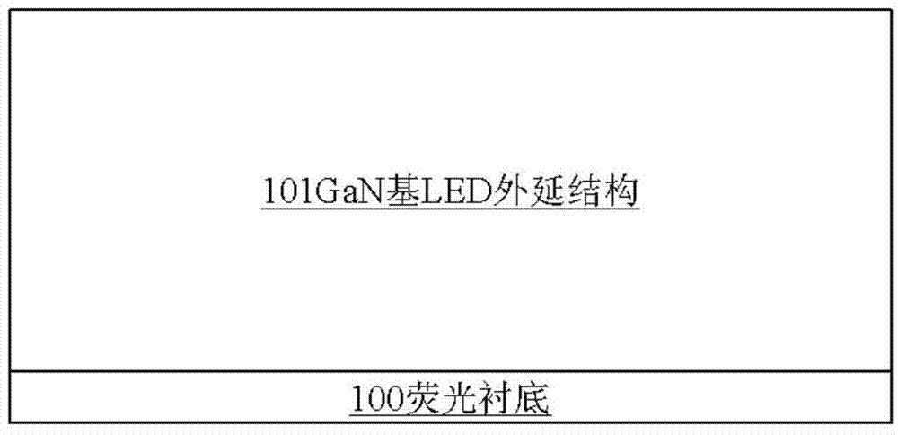
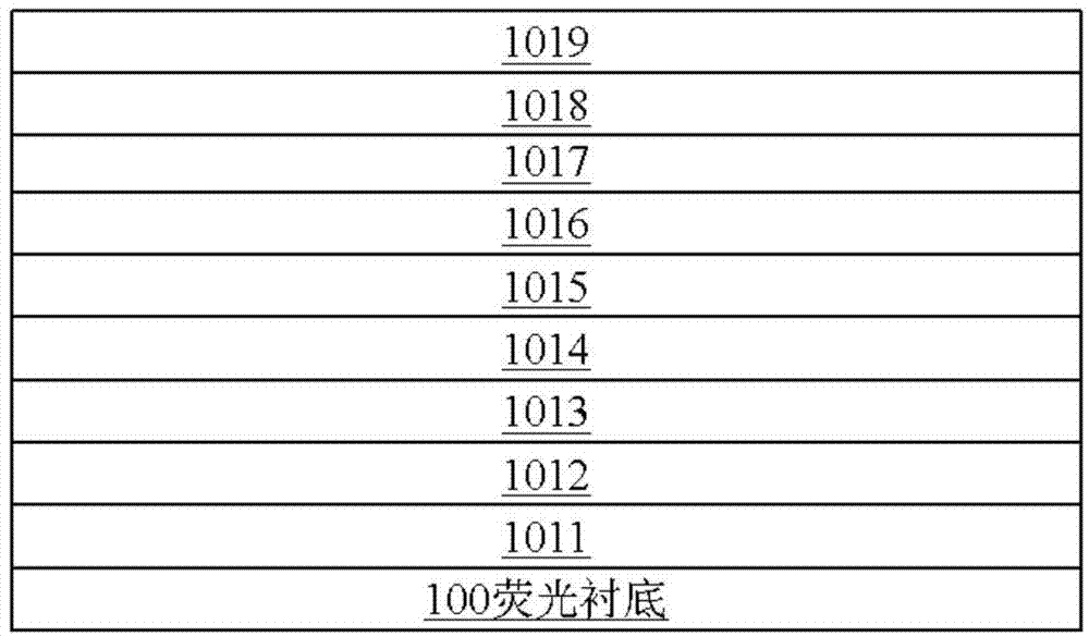
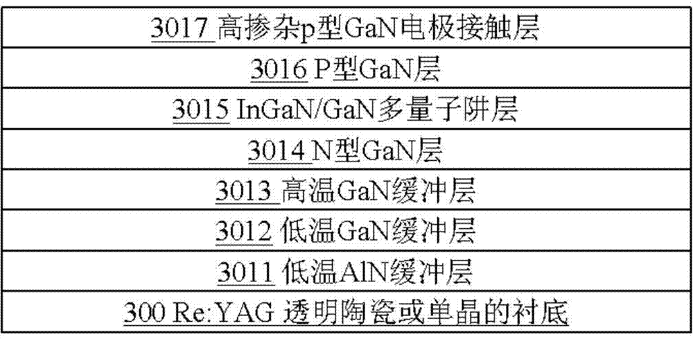
[0048] 0.005wt.% Ce 2 o 3 The powder is mixed into the YAG powder, fully mixed by wet ball milling, and dried to obtain the fluorescent ceramic powder raw material. The fluorescent ceramic powder raw material is formed into an embryo body by cold isostatic pressing. Put the green body into a vacuum high-temperature sintering furnace, the sintering temperature is 1450°C, and the sintering time is 10 hours. The thickness of the sintered transparent ceramic sample is 600 μm after thinning and surface fine polishing, and the surface roughness is 3 nm. Put this Ce:YAG transparent ceramic material as the substrate into the metal organic compound chemical vapor deposition equipment, perform high-temperature cleaning treatment in a hydrogen atmosphere at 800°C for 20 minutes, then drop the temperature to 500°C, and grow a low-temperature AlN buffer layer with a thickness of 15nm; continue Grow a low-temperature GaN buffer layer with a thickness of 300nm; increase the temperature to...
Embodiment 2
[0050] 0.3wt.% Ce 2 O, the powder is blended into YAG powder, fully mixed by wet ball milling, and the fluorescent ceramic powder raw material is obtained after drying. The fluorescent ceramic powder raw material is formed into an embryo body by cold isostatic pressing. Put the green body into a vacuum high-temperature sintering furnace, the sintering temperature is 1850°C, and the sintering time is 15 hours. The sintered transparent ceramic sample has a thickness of 450 μm and a surface roughness of 2 nm after thinning and surface fine polishing. Put the Ce:YAG ceramic material as the substrate into the metal organic compound chemical vapor deposition equipment, perform high-temperature cleaning treatment in a hydrogen atmosphere at 1400°C for 20 minutes, then drop the temperature to 700°C, and grow a low-temperature AlN buffer layer with a thickness of 60nm; continue to grow 50nm thick low-temperature GaN buffer layer; raise the temperature to 1200°C to grow a 4μm-thick hi...
Embodiment 3
[0052] 1.2wt.% Gd 2 o 3 powder with 25wt.% Gd 2 o 3 Blended into YAG powder, fully mixed by wet ball milling, and dried to obtain fluorescent ceramic powder raw materials. The fluorescent ceramic powder raw material is formed into an embryo body by cold isostatic pressing. Put the green body into a vacuum high-temperature sintering furnace, the sintering temperature is 1830°C, and the sintering time is 12 hours. The sintered transparent ceramic sample has a thickness of 350 μm and a surface roughness of 1 nm after thinning and surface fine polishing. Put the Ce:YAG ceramic material as the substrate into the metal organic compound chemical vapor deposition equipment, perform high-temperature cleaning treatment in a hydrogen atmosphere at 1300°C for 15 minutes, then drop the temperature to 500°C, and grow a low-temperature AlN buffer layer with a thickness of 60nm; To 700°C, grow a 50nm-thick low-temperature GaN buffer layer; raise the temperature to 1100°C, grow a 4μm-thic...
PUM
| Property | Measurement | Unit |
|---|---|---|
| Roughness | aaaaa | aaaaa |
| Surface roughness | aaaaa | aaaaa |
Abstract
Description
Claims
Application Information
 - R&D
- Intellectual Property
- Life Sciences
- Materials
- Tech Scout
- Unparalleled Data Quality
- Higher Quality Content
- 60% Fewer Hallucinations
Browse by: Latest US Patents, China's latest patents, Technical Efficacy Thesaurus, Application Domain, Technology Topic, Popular Technical Reports.
© 2025 PatSnap. All rights reserved.Legal|Privacy policy|Modern Slavery Act Transparency Statement|Sitemap|About US| Contact US: help@patsnap.com


