Laser machining method for fine scribing structure at ceramic surface
A laser processing method and ceramic surface technology, which is applied in the field of ceramic surface processing, can solve the problems of line width precision limitation, etc., and achieve the effect of low cost, uniform line diameter and simple operation
- Summary
- Abstract
- Description
- Claims
- Application Information
AI Technical Summary
Problems solved by technology
Method used
Image
Examples
Embodiment Construction
[0027] In order to make the object, technical solution and advantages of the present invention clearer, the implementation manner of the present invention will be further described in detail below in conjunction with the accompanying drawings.
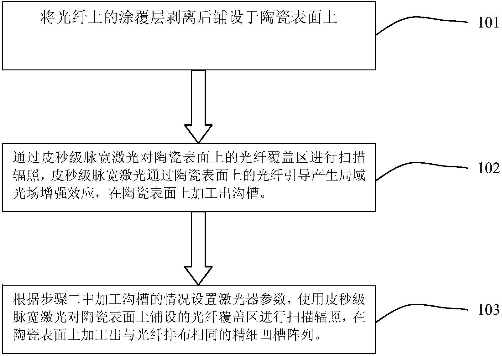
[0028] The invention provides a method for realizing a fine scribe line structure on the ceramic surface by using an optical fiber to guide a picosecond-level pulse width laser. Such as figure 1 Shown: described method comprises the steps:
[0029] [101] Peel off the coating layer on the single-mode optical fiber and lay it on the ceramic surface, in a single laying or multiple close-packed way;
[0030] [102] Scanning the optical fiber coverage area on the ceramic surface with a picosecond pulse width laser, the picosecond pulse width laser generates a local light field enhancement effect under the guidance of the optical fiber on the ceramic surface, and processes grooves; The distance from the ceramic surface to the focal point of...
PUM
 Abstract
Description
Claims
Application Information
 - R&D
- Intellectual Property
- Life Sciences
- Materials
- Tech Scout
- Unparalleled Data Quality
- Higher Quality Content
- 60% Fewer Hallucinations
Browse by: Latest US Patents, China's latest patents, Technical Efficacy Thesaurus, Application Domain, Technology Topic, Popular Technical Reports.
© 2025 PatSnap. All rights reserved.Legal|Privacy policy|Modern Slavery Act Transparency Statement|Sitemap|About US| Contact US: help@patsnap.com


