Doped gan thin film grown on strontium aluminate tantalum lanthanum substrate and preparation method thereof

A strontium tantalum lanthanum aluminate and thin film technology is applied in the field of doped GaN thin films and their preparation, which can solve the problems of insufficient luminous efficiency of LED chips, affecting the performance of GaN-based devices, reducing material carrier mobility, and the like. Repeatability, suppression of interfacial reactions, effect of low film dislocation density

Active Publication Date: 2015-10-28
SOUTH CHINA UNIV OF TECH
View PDF4 Cites 0 Cited by
  • Summary
  • Abstract
  • Description
  • Claims
  • Application Information

AI Technical Summary

Problems solved by technology

Although the luminous efficiency of LED has surpassed that of fluorescent lamps and incandescent lamps, the luminous efficiency of commercial LEDs is still lower than that of sodium lamps (150lm / W), and the price per lumen / watt is relatively high.
At present, the luminous efficiency of LED chips is not high enough, one of the main reasons is that the sapphire substrate causes
Since the lattice mismatch between sapphire and GaN is as high as 17%, a high dislocation density is formed during the epitaxial GaN film process, which reduces the carrier mobility of the material and shortens the carrier lifetime, which in turn affects the GaN substrate. Device performance
Secondly, due to the thermal expansion coefficient of sapphire at room temperature (6.63×10 -6 K -1 ) compared with the thermal expansion coefficient of GaN (5.6×10 -6 K -1 ) is large, and the thermal mismatch between the two is about -18.4%. When the epitaxial layer growth is completed, the device will generate a large compressive stress during the process of cooling the device from the high temperature of the epitaxial growth to room temperature, which will easily lead to the torsion of the film and the substrate. crack
Third, due to the low thermal conductivity of sapphire (25W / m.K at 100°C), it is difficult to discharge the heat generated in the chip in time, resulting in heat accumulation, which reduces the internal quantum efficiency of the device and ultimately affects the performance of the device

Method used


Image

  • Doped gan thin film grown on strontium aluminate tantalum lanthanum substrate and preparation method thereof
  • Doped gan thin film grown on strontium aluminate tantalum lanthanum substrate and preparation method thereof
  • Doped gan thin film grown on strontium aluminate tantalum lanthanum substrate and preparation method thereof

Examples


Embodiment 1

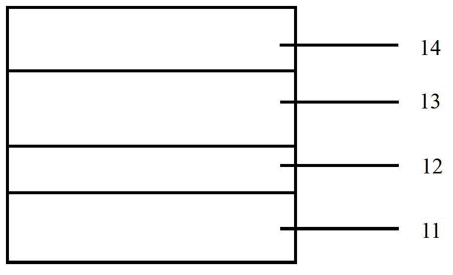
[0035] In this embodiment, the method for preparing a doped GaN thin film grown on a strontium aluminate tantalum lanthanum substrate includes the following steps:

[0036] (1) Selection of substrate and its crystal orientation: (1) Selection of substrate and its crystal orientation: La 0.x Sr 1.7 AlTaO 6 The substrate, with the (111) plane offset from the (100) direction by 0.5° as the epitaxial plane, the crystal epitaxial orientation relationship is: the (0001) plane of GaN is parallel to the La 0.3 Sr 1.7 AlTaO 6 The (111) plane of GaN(0001) / / La 0.3 Sr 1.7 AlTaO 6 (111);

[0037] (2) Surface polishing, cleaning, and annealing of the substrate. The specific process of the annealing is: put the substrate into the annealing chamber, and treat La 0.3 Sr 1.7 AlTaO 6 The substrate was annealed for 3 hours and then air-cooled to room temperature;

[0038] The surface polishing of the substrate is specifically:

[0039] La 0.3 Sr 1.7 AlTaO 6 The surface of the subst...

Embodiment 2

[0050] In this embodiment, the method for preparing a doped GaN thin film grown on a strontium aluminate tantalum lanthanum substrate includes the following steps:

[0051] (1) Selection of substrate and its crystal orientation: (1) Selection of substrate and its crystal orientation: La 0.3 Sr 1.7 AlTaO 6 The substrate, with the (111) plane offset from the (100) direction by 1° as the epitaxial plane, the crystal epitaxial orientation relationship is: the (0001) plane of GaN is parallel to the La 0.3 Sr 1.7 AlTaO 6 (111) side;

[0052] (2) Surface polishing, cleaning, and annealing of the substrate. The specific process of the annealing is: put the substrate into the annealing chamber, and treat La 0.3 Sr 1.7 AlTaO 6 The substrate was annealed for 5 hours and then air-cooled to room temperature;

[0053] The surface polishing of the substrate is specifically:

[0054] La 0.3 Sr 1.7 AlTaO 6 The surface of the substrate is polished with diamond slurry, and the surfac...

Embodiment 3

[0064] In this embodiment, except the following features, all the other features are the same as in Embodiment 1:

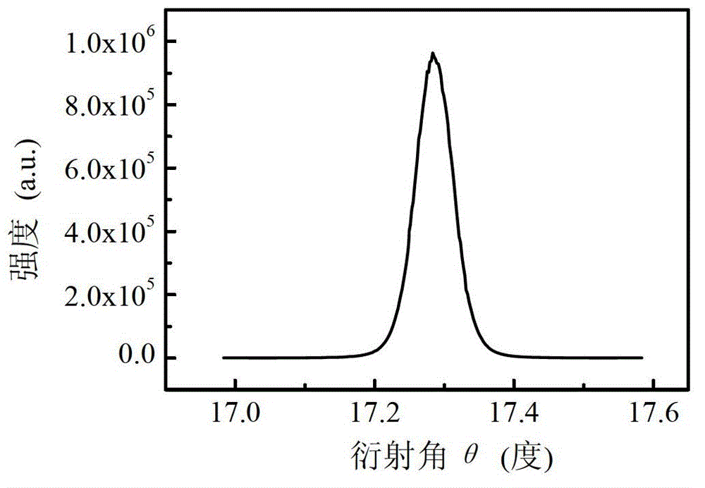
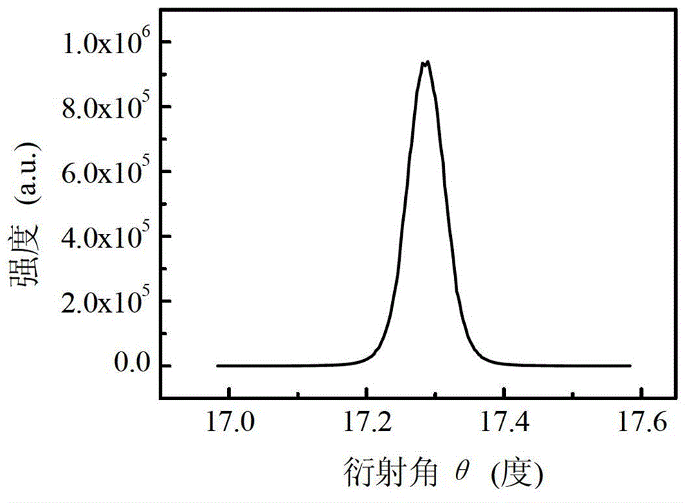
[0065] The growth process of n-type doped GaN film is as follows: using molecular beam epitaxy growth process, the substrate temperature is raised to 750°C, and the reaction chamber pressure is 6.0×10 -5 Pa, V / III value is 50, and Si is used as n-type dopant source, and the growth rate is 0.8ML / s. The electron concentration of the n-type doped GaN film prepared in this example is 6×10 18 cm -3 , with an electron mobility of 310 cm 2 / v·s.


PUM

PropertyMeasurementUnit
thicknessaaaaaaaaaa
thicknessaaaaaaaaaa
thicknessaaaaaaaaaa

Abstract

The invention discloses a doped GaN film growing on a La0.3Sr1.7AlTaO6 substrate. The doped GaN film comprises a GaN buffer layer growing on the La0.3Sr1.7AlTaO6 substrate, an undoped GaN layer growing on the GaN buffer layer and a doped GaN film growing on the undoped GaN layer. The doped GaN film is an n-type doped GaN film or a p-type doped GaN film. The invention further discloses a manufacturing method of the doped GaN film growing on the La0.3Sr1.7AlTaO6 substrate. Compared with the prior art, the doped GaN film growing on the La0.3Sr1.7AlTaO6 substrate and the manufacturing method of the doped GaN film have the advantages of simple growing process and low manufacturing cost. Besides, the manufactured n-type or p-type doped film has low defect density, good crystallization quality and optical property.

Description

technical field [0001] The invention relates to a doped GaN thin film and a preparation method thereof, in particular to a film grown on strontium aluminate tantalum lanthanum (La 0.3 Sr 1.7 AlTaO 6 ) doped GaN thin film on substrate and its preparation method. Background technique [0002] Light-emitting diode (LED), as a new type of solid-state lighting source and green light source, has outstanding features such as small size, low power consumption, environmental protection, long service life, high brightness, low heat and colorful, and is widely used in outdoor lighting, commercial lighting and decoration Engineering and other fields have a wide range of applications. At present, under the background of the increasingly serious problem of global warming, saving energy and reducing greenhouse gas emissions has become an important issue faced by the whole world. A low-carbon economy based on low energy consumption, low pollution, and low emissions will become an import...

Claims


Application Information

Patent Timeline
Patent Type & Authority Patents(China)
IPC IPC(8): H01L33/02H01L33/12
Inventor 李国强王文樑杨为家刘作莲林云昊
Owner SOUTH CHINA UNIV OF TECH
Why Eureka
Try Eureka