Laser doping technique used for improving adhesive force between metal electrode and crystalline silicon

A technology of laser doping and metal electrodes, which is applied in the field of laser doping technology, can solve problems affecting doping uniformity, battery performance, laser damage, etc., to meet industrial mass production, improve performance and stability, and improve The effect of conversion efficiency

Inactive Publication Date: 2013-02-06
ALTUSVIA ENERGY TAICANG
View PDF2 Cites 6 Cited by
  • Summary
  • Abstract
  • Description
  • Claims
  • Application Information

AI Technical Summary

Problems solved by technology

[0005] However, this process method has an important disadvantage, that is: after the silicon wafer is laser doped and electroplated, the adhesion between the metal electrode formed after electroplating and the crystalline silicon is very low, which becomes a very important factor affecting the stability and reliability of the battery. , which limits its industrial mass production, although the industry also mentions that the low adhesion can be avoided by increasing the laser energy to increase the surface roughness of silicon, such as using higher surface roughness for electroplating to form a firm metal electrode and silicon-based contact .As mentioned in the open literature "Influence of laser power on the properties of silicon solar cells" Author: Z.Hameiri et al published in Solar Energy materials & solar cell 95 (2011) 1085-1094, however, the method of increasing laser energy The formation itself will cause laser damage, and at the same time reduce the conversion efficiency of the battery and affect the performance of the battery
[0006] In fact, the low adhesion between metal and silicon itself has a lot to do with the laser doping process. On the one hand, if figure 2 The diameter of the Gaussian spot 22 formed after the focused laser is shown is very small, usually only 10-15um. During the high-speed scanning process of the laser, due to the uneven energy distribution of the focused Gaussian spot, the temperature gradient of the spot along the central area and the peripheral area is too large. There will be multiple alternating cycles of high and low temperature gradients in the overlapping area of ​​the spot in the scanning direction, which will affect the uniformity of doping and the uniformity of contact between the metal and the silicon substrate after electroplating. On the other hand, the time distribution of laser energy is not optimal. The laser radiates energy to the surface of the material in a pulsed manner. Due to the different thermal and physical parameters of the passivation layer, the dopant source and the silicon-based material, the melting point of the passivation layer is much higher than that of the dopant source. When the passivation layer and the silicon base melt, Most of the dopant source coated on the surface of the silicon base has been vaporized. Only a small part can diffuse smoothly to the surface of the crystalline silicon, which also leads to a great impact on the uniformity of the doping, which is not conducive to the subsequent high-quality electroplating process

Method used


Image

  • Laser doping technique used for improving adhesive force between metal electrode and crystalline silicon
  • Laser doping technique used for improving adhesive force between metal electrode and crystalline silicon
  • Laser doping technique used for improving adhesive force between metal electrode and crystalline silicon

Examples


Embodiment 1

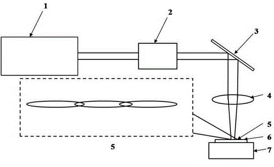
[0023] Such as figure 1 As shown, a laser doping process for improving the adhesion between metal electrodes and crystalline silicon includes the following steps:

[0024] (1) Silicon wafer texturing: selection, p-type monocrystalline silicon wafer as the base material and texturing;

[0025] (2) Boron diffusion: After the silicon wafer is cleaned, put the silicon wafer face to face into the diffusion furnace for boron diffusion;

[0026] (3) Growth mask: SiNx and SiOx laminated anti-reflection passivation film is used on the front of the silicon wafer, and aluminum paste is printed on the back of the silicon wafer and sintered;

[0027] (4) spin-coated phosphoric acid;

[0028] (5) Laser doping: The processing of silicon wafers is completed by using a focused linear spot optical system combined with a shaped pulse wave. The focused linear optical system includes a laser 1, an optical shaping system 2, a mirror 3, and a focusing lens 4. platform 7, the laser 1 is connected...

Embodiment 2

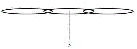
[0031] Such as figure 1 The focusing linear spot optical system used in the shown laser doping, the focusing linear optical system includes a laser 1, an optical shaping system 2, a mirror 3, a focusing lens 4, a workbench 7, and the laser 1 and Described optical shaping system 2 is connected, and described mirror 3 is arranged before described optical shaping system 2 and described focusing lens 4, and described workbench 7 is arranged at the below of focusing lens 4, and described The laser 1 emits the reshaped focused linear spot 5 through the optical shaping system 2, and the focused linear spot 5 is projected onto the focusing lens 4 through the mirror 3, and the focused linear spot 5 of the focusing lens 4 is placed on the workbench The silicon wafer 6 on 7 is processed, and the silicon wafer 6 moves with the workbench 7, and the focused linear light spot 5 acts on the surface of the silicon wafer 6. The ratio of the short axis and the long axis of the focused linear li...


PUM


Abstract

The invention discloses a laser doping technique used for improving the adhesive force between a metal electrode and a crystalline silicon. The laser doping technique comprises wool making on a silicon wafer, boron diffusion, mark growing, laser doping and electroplating. In the laser doping technique, linear focus light spots with uniform energy distribution are adopted, and the control on the waveforms of pulses is combined, so that after the laser is doped, the texturing appearance of the surface of the silicon can be kept, the uniform doping concentration distribution can be formed, thereby effectively improving the adhesive force between the electroplated metal electrode and the crystalline silicon; in addition, according to the method, the performance and the stability of a battery can be improved, and the battery conversion efficiency is improved, so as to meet the industrial production in a large scale.

Description

technical field [0001] The invention relates to the manufacture of crystalline silicon solar cells, in particular to a laser doping process for improving the adhesion between metal electrodes and crystalline silicon. Background technique [0002] The industrial production of modern solar cells is developing towards high efficiency and low cost. Lasers have decades of history in solar cell manufacturing, including early buried grid grooves (LGBC), laser edge cutting, drilling (EWT and MWT) and laser Doping, among them, the use of laser doping technology to manufacture selective emitter solar cells can significantly improve the conversion efficiency of solar cells, and at the same time reduce the cost of cell manufacturing, which has become a technology with great potential for industrial production. [0003] The use of laser doping combined with electroplating technology to manufacture batteries developed by the University of New South Wales in Australia is a method with low ...

Claims


Application Information

Patent Timeline
Patent Type & Authority Applications(China)
IPC IPC(8): H01L31/18H01L31/0224
CPCY02P70/50
Inventor 吴亚军冯立学梁会宁胡元庆李华恩
Owner ALTUSVIA ENERGY TAICANG
Why Eureka
Try Eureka