Transparent conductive films
- Summary
- Abstract
- Description
- Claims
- Application Information
AI Technical Summary
Problems solved by technology
Method used
Image
Examples
Embodiment
[0114] Hereinafter, the present invention will be described in more detail using examples of the present invention, but the present invention is not limited to these examples.
[0115] [Evaluation of basic properties of transparent conductive films]
[0116] The composition of the obtained transparent conductive film was analyzed by ICP emission spectroscopy. The film thickness of the transparent conductive film was measured with a surface roughness meter (manufactured by Tencor, Alpha-Step IQ). The film formation rate was calculated from the film thickness and film formation time.
[0117] The surface resistance of the film was measured by a four-probe method using a resistivity meter (LORESTA EP MCP-T360 manufactured by DIA Instruments). The resistivity of the film was calculated from the product of the surface resistance of the film and the film thickness. The carrier electron concentration and mobility of the film were determined by Hall effect measurement. The refract...
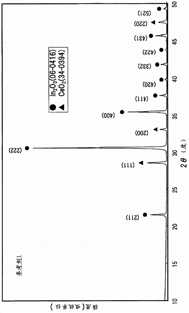
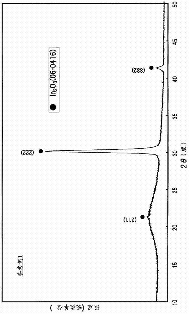
reference example 1)
[0121] Indium oxide powder and cerium oxide powder were adjusted to have an average particle diameter of 1 μm or less as raw material powders. These powders were prepared so that the cerium content was 9 atomic % in terms of Ce / (In+Ce) atomic ratio, they were put into a resin pot together with water, and mixed with a wet ball mill. At this time, using hard ZrO 2 balls, set the mixing time to 18 hours. After mixing, the slurry is taken out, filtered, dried and granulated. Apply 3 ton / cm with a cold isostatic press 2 The pressure will shape the granules.
[0122] Next, at every 0.1m 3 The molded body was sintered at a sintering temperature of 1400° C. for 20 hours in an atmosphere in which oxygen was introduced into the atmosphere in the sintering furnace at a rate of 5 liters / minute in the furnace volume. At this time, the temperature was raised at 1°C / min, the introduction of oxygen was stopped during cooling after sintering, and the temperature was lowered to 1000°C at 1...
reference example 2)
[0131] A transparent conductive film was formed in the same manner as in Reference Example 1, except that a sputtering target composed of an oxide sintered body having a cerium content of 7 atomic % in Ce / (In+Ce) atomic ratio was used. It was confirmed that the composition of the obtained transparent conductive film was almost the same as that of the target.
[0132] The resistivity of the film was measured and the result was 5.9×10 -4 Ωcm. In addition, the Hall effect measurement was performed, and the carrier electron concentration was 2.5×10 20 cm -3 , the carrier electron mobility is 42cm 2 V -1 the s -1 . The refractive index at a wavelength of 460 nm is 2.20. As a result of analyzing the crystallinity of the film by X-ray diffraction measurement, it was confirmed that it was a crystalline film composed only of an indium oxide phase with a bixbyite structure. The surface roughness of the film was measured by AFM, and the arithmetic mean height Ra was 1.3 nm.
[0...
PUM
| Property | Measurement | Unit |
|---|---|---|
| height | aaaaa | aaaaa |
| electrical resistivity | aaaaa | aaaaa |
| electrical resistivity | aaaaa | aaaaa |
Abstract
Description
Claims
Application Information
 - R&D
- Intellectual Property
- Life Sciences
- Materials
- Tech Scout
- Unparalleled Data Quality
- Higher Quality Content
- 60% Fewer Hallucinations
Browse by: Latest US Patents, China's latest patents, Technical Efficacy Thesaurus, Application Domain, Technology Topic, Popular Technical Reports.
© 2025 PatSnap. All rights reserved.Legal|Privacy policy|Modern Slavery Act Transparency Statement|Sitemap|About US| Contact US: help@patsnap.com


