
Radio-frequency integrated band-pass filter with impedance match

A band-pass filter, radio frequency integration technology, applied in impedance networks, electrical components, multi-terminal-to-network, etc., can solve problems such as increasing power consumption, increasing system costs, and difficulty in reaching receiver systems, and achieving improved quality factor, The effect of saving PCB area

Active Publication Date: 2012-02-01
锐立平芯微电子(广州)有限责任公司
View PDF2 Cites 23 Cited by
  • Summary
  • Abstract
  • Description
  • Claims
  • Application Information

AI Technical Summary

Problems solved by technology

Only the RF bandpass filter, due to its high operating frequency, has strict requirements on insertion loss and noise figure, and it is difficult for the on-chip RF bandpass filter realized by CMOS technology to meet the requirements of the receiver system. Therefore, currently The common practice is to use a high-performance off-chip SAW (Surface Acoustic Wave) bandpass filter
Obviously, this approach is not conducive to the miniaturization and low cost of the system, especially for mobile communication devices with multiple communication modes and supporting multiple frequency bands, multiple off-chip bandpass filters of different frequency bands are required, so that not only The volume of the system becomes very large, and the cost of the system is increased, and the power consumption is increased

Method used


Image

  • Radio-frequency integrated band-pass filter with impedance match
  • Radio-frequency integrated band-pass filter with impedance match
  • Radio-frequency integrated band-pass filter with impedance match

Examples


Embodiment Construction

[0018] The principles and features of the present invention are described below in conjunction with the accompanying drawings, and the examples given are only used to explain the present invention, and are not intended to limit the scope of the present invention.

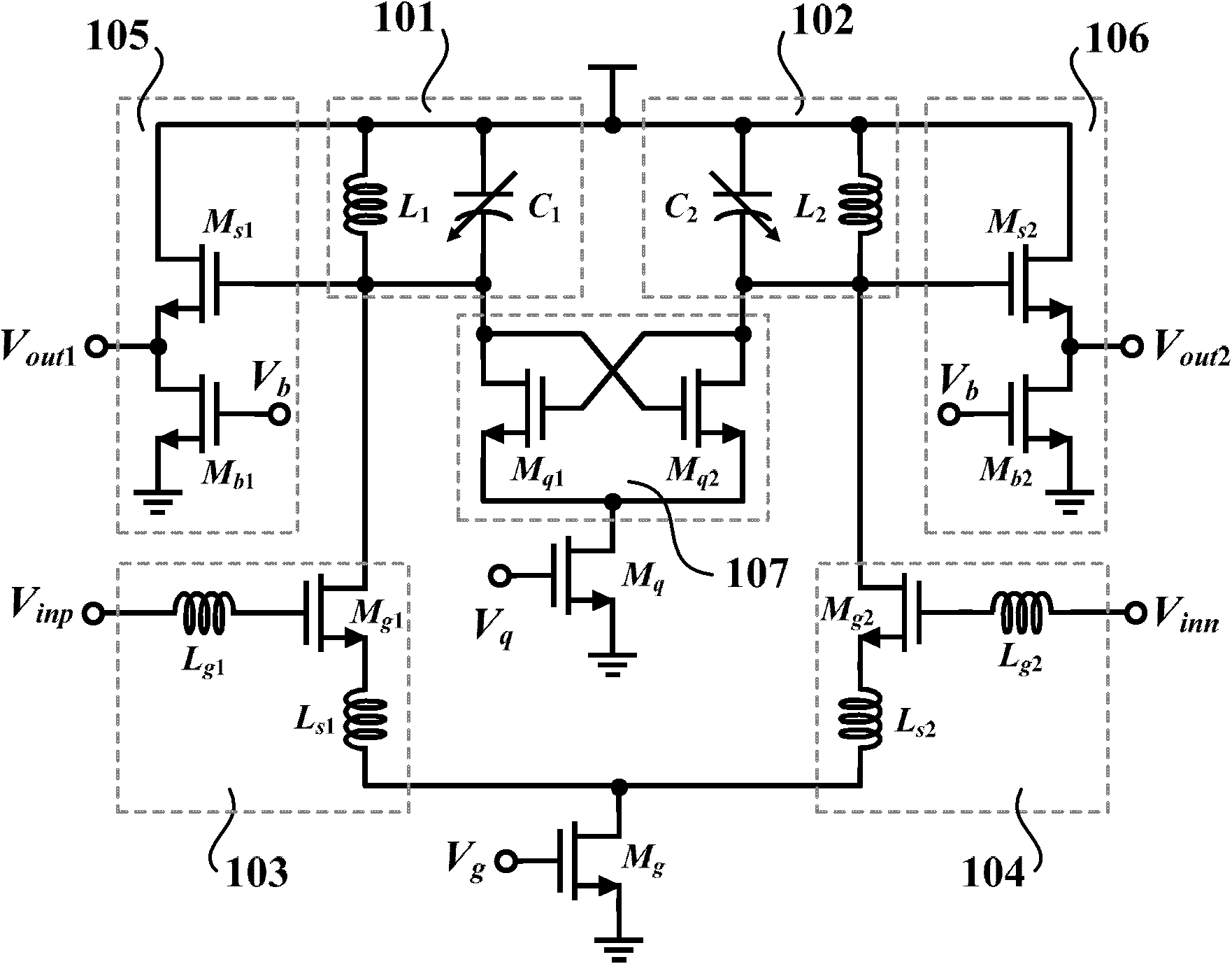
[0019] figure 1 It is a schematic circuit diagram of the radio frequency integrated bandpass filter with impedance matching of the present invention. Such as figure 1 As shown, the RF integrated bandpass filter with impedance matching includes a first LC resonant tank 101, a second LC resonant tank 102, a first input impedance matching circuit 103, a second input impedance matching circuit 104, a first output impedance Matching circuit 105, second output impedance matching circuit 106, active negative resistance compensation circuit 107, first NMOS tail current transistor M g and a second NMOS tail current transistor M q ; The first LC resonant circuit 101 is connected to the second LC resonant circuit 102; the f...


PUM


Abstract

The invention relates to a radio-frequency integrated band-pass filter with impedance match, belonging to the technical field of design of integrated circuits. Based on a CMOS (Complementary Metal-Oxide-Semiconductor Transistor) process, by utilizing an active negative resistance compensation technology, the radio-frequency integrated band-pass filter with the impedance match is composed of two LC (Inductance-Capacitance) resonance circuits, two input impedance match circuits, two output impedance match circuits, an active negative resistance compensation circuit and two NMOS (N-channel Metal Oxide Semiconductor) tail current transistors, wherein the two LC resonance circuits, the two input impedance match circuits and the two output impedance match circuits have the same connection way and symmetrical structures. The adjustment on the central frequency, the band-pass gain and the bandwidth of the band-pass filter can be realized through adjusting a bias voltage of a varactor and adjusting bias voltages of two NMOS tail current transistor grids. The radio-frequency integrated band-pass filter provided by the invention not only can carry out integration on a chip by adopting the CMOS process, but also is provided with an input-output impedance match circuit on the chip, and discrete devices out of the chip are not needed, so that the integration level is greatly improved and a feasible scheme for realizing single chip integration is supplied to a radio-frequency front end of a wireless receiver.

Description

technical field [0001] The invention relates to a radio frequency integrated bandpass filter with impedance matching, belonging to the technical field of integrated circuit design. Background technique [0002] In recent years, with the rapid development of the wireless communication market, the requirements for low cost and miniaturization of mobile communication equipment such as mobile phones, GPS navigation equipment, and electronic medical equipment are getting higher and higher. As the most important radio frequency front-end module in the mobile communication system, it is also developing towards the SoC direction to meet the requirements of low cost and miniaturization of the system. [0003] In the mobile communication system, the RF front-end module is used to modulate the transmitted signal and demodulate the received signal. Taking the RF front-end module in the receiver as an example, its composition includes a low-noise amplifier, a mixer, a frequency synthesiz...

Claims


Application Information

Patent Timeline
IPC IPC(8): H03H7/12
Inventor 刘欣张海英赵磊
Owner 锐立平芯微电子(广州)有限责任公司
Learn More