Preparation technique of SiGe Bi-CMOS appliance

A preparation process and device technology, applied in the field of process integration of germanium-silicon Bi-CMOS devices, can solve problems such as large-area exposure, device characteristic changes, development, etc., to reduce process defects, simplify process flow, improve yield and reliability. sexual effect

Active Publication Date: 2011-01-05
SHANGHAI HUAHONG GRACE SEMICON MFG CORP
View PDF0 Cites 6 Cited by
  • Summary
  • Abstract
  • Description
  • Claims
  • Application Information

AI Technical Summary

Problems solved by technology

However, when forming Si / Ge devices, in order to remove the protective layer in the Si / Ge region, the subsequent Si / Ge epitaxial growth is performed. At this time, from the perspective of the layout, all Si / Ge device regions will be opened, and the Si / Ge device The area is much larger than CMOS, so a large area exposure is required, and developing defects are prone to occur at this time
The subsequent Si / Ge epitaxial process is a very strict molecular epitaxial growth along the crystal direction, and any small defects will cause lattice defects and cause changes in device characteristics.

Method used


Image

  • Preparation technique of SiGe Bi-CMOS appliance
  • Preparation technique of SiGe Bi-CMOS appliance
  • Preparation technique of SiGe Bi-CMOS appliance

Examples


Embodiment Construction

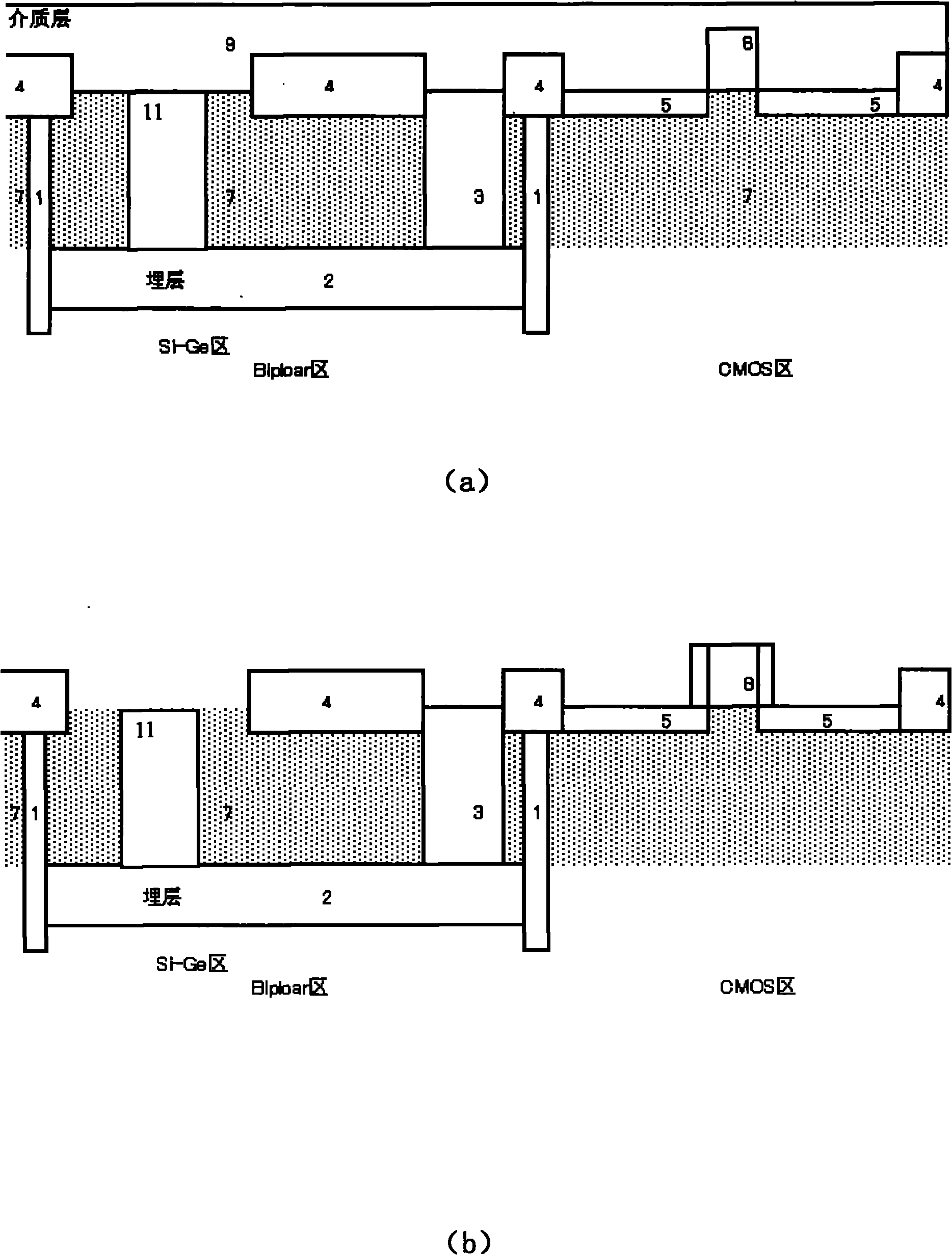
[0028] Such as Figure 4 As shown, the silicon germanium Bi-CMOS device preparation process of the present invention comprises the following steps when forming the sidewall and the metal silicide barrier layer of the silicon germanium Bi-CMOS device:

[0029] Firstly, the substrate and the doped region of a conventional SiGe device are formed on a silicon substrate, including the buried layer 2 in the SiGe bipolar region, and the deep trench isolation 1 separates the epitaxial layer 7, including the collector electrode 11 of the device, The collector lead-out region 3 , the shallow trench isolation 4 , and the gate 8 of the CMOS device, or in some cases, LDD and source-drain implantation can be completed first to form the source-drain region 5 .

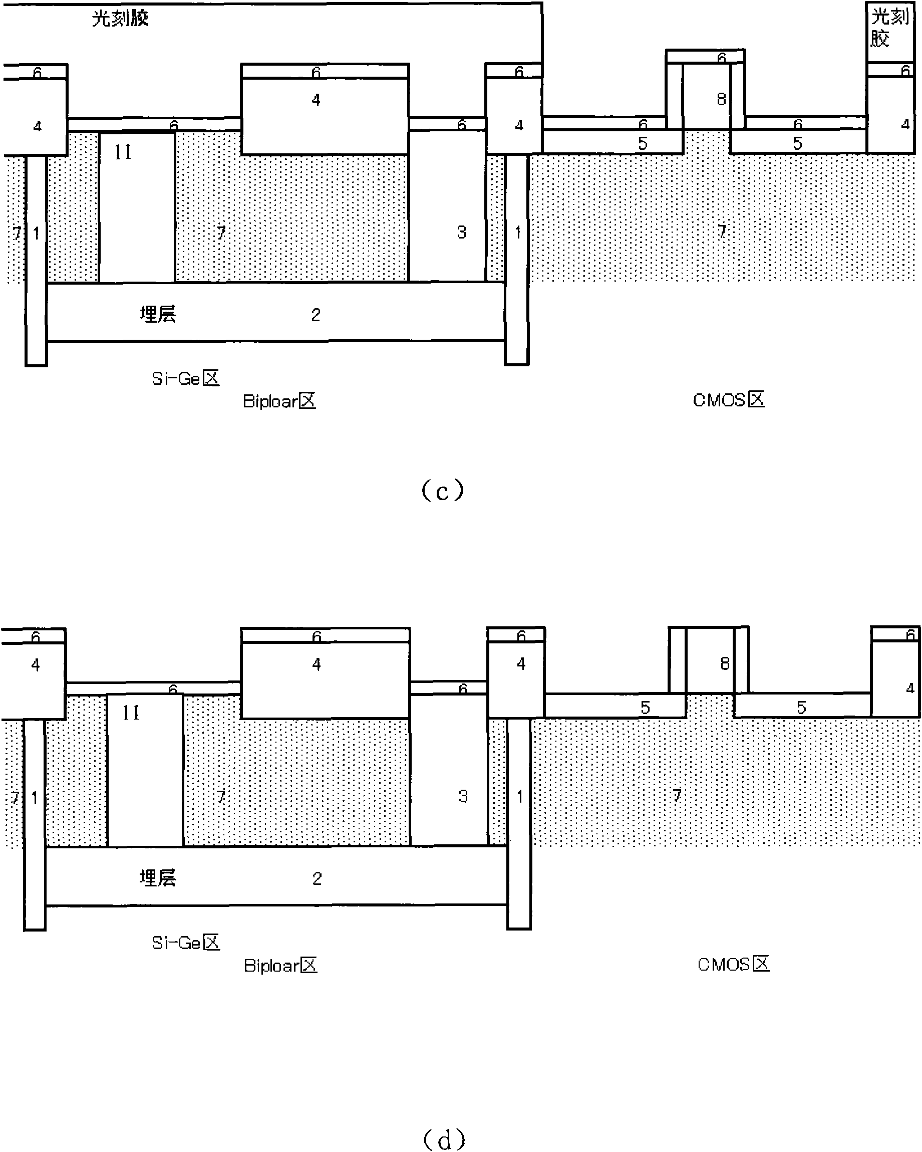
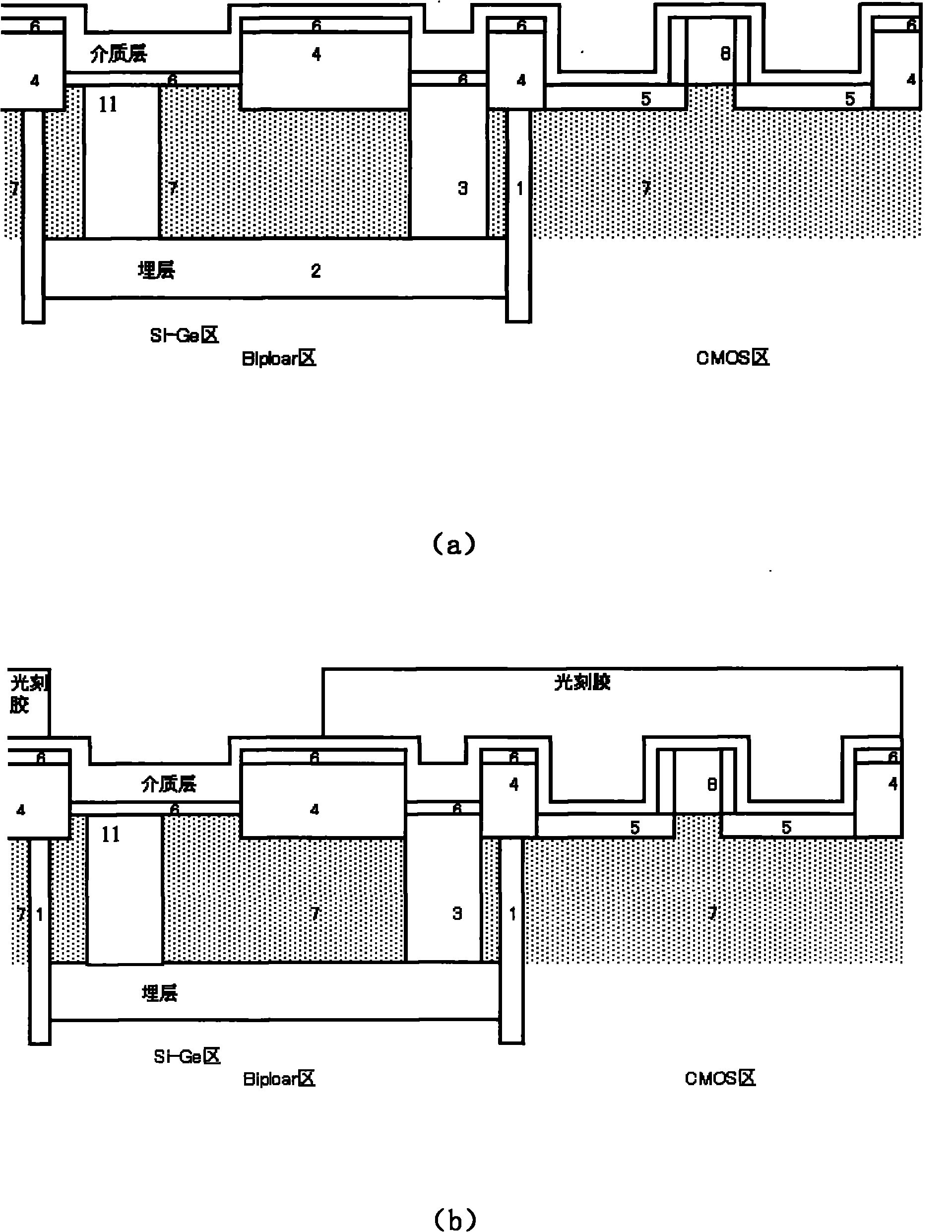
[0030] Such as image 3 As shown in (a), a dielectric film layer is deposited over the entire silicon germanium device and CMOS device, and the dielectric film can be an oxide (such as SiO 2 ) or nitrides (such as SiN), there are a...


PUM


Abstract

The invention discloses a preparation technique of a SiGe Bi-CMOS appliance. The step of forming a side wall and a metallic silicide barrier layer of the SiGe Bi-CMOS appliance comprises the following steps of: 1, depositing a dielectric film layer; 2, spin-coating a negative photoresist; 3, exposing with a photomask of the metallic silicide barrier layer to form a metallic silicide barrier layer pattern; 4, etching to form the side wall and removing the dielectric film layer on the non-metallic silicide barrier layer at the same time; 5, growing the dielectric film layer protecting the CMOS appliance; 6, photoetching and etching to open a Si/Ge growth zone; and 7, performing the subsequent Si/Ge appliance forming process. In the invention, the side wall and the metallic silicide barrier layer are formed through photolithography at one time by photoetching the metallic silicide barrier layer with the negative photoresist, so that the process flow is simplified and the yield and reliability of the appliance are improved.

Description

technical field [0001] The invention relates to the field of semiconductor integrated circuit technology, in particular to a process integration method for silicon germanium Bi-CMOS (Bipolar Complementary Metal Oxide Semiconductor, Bipolar Complementary Metal Oxide Semiconductor) devices in the field of semiconductor technology. Background technique [0002] In semiconductor manufacturing, because the energy band gap of Si / Ge is smaller than that of Si, the recombination speed of electron / hole pairs is faster, which can be applied to high-speed devices. At the same time, the Si / Ge device process is highly compatible with the existing Si integrated circuit process. Ge-Si bipolar (Bipolar) device is a relatively commonly used analog device. At the same time, in order to improve the integration level, people integrate the corresponding bipolar devices and metal oxide complementary semiconductor (CMOS) devices together to form germanium silicon Bi-CMOS devices, which are widely...

Claims


Application Information

Patent Timeline
Patent Type & Authority Applications(China)
IPC IPC(8): H01L21/8249G03F7/038
Inventor 王雷
Owner SHANGHAI HUAHONG GRACE SEMICON MFG CORP
Why Eureka
Try Eureka