Transparent conducting film and preparation method thereof, solar battery and flat panel display device

A technology of transparent conductive film and manufacturing method, applied in semiconductor/solid-state device manufacturing, final product manufacturing, sustainable manufacturing/processing, etc., can solve the problem of long process time, affecting film performance, and difficulty in maintaining stable grain orientation of zinc oxide film and other problems, to achieve uniform suede structure, improve photoelectric conversion efficiency, and good light absorption.

Active Publication Date: 2014-02-12
BEIJING NAURA MICROELECTRONICS EQUIP CO LTD
View PDF6 Cites 0 Cited by
  • Summary
  • Abstract
  • Description
  • Claims
  • Application Information

AI Technical Summary

Problems solved by technology

[0007] The disadvantage of the solution disclosed in the above-mentioned Chinese patent application documents is that the thickness of the zinc oxide film used as the front electrode of the thin-film solar cell is generally greater than or equal to 800nm, the process time required for the above-mentioned solution will be very long, and the grain orientation of the zinc oxide film during the thickening process Difficult to maintain stability, affecting final membrane performance

Method used


Image

  • Transparent conducting film and preparation method thereof, solar battery and flat panel display device
  • Transparent conducting film and preparation method thereof, solar battery and flat panel display device
  • Transparent conducting film and preparation method thereof, solar battery and flat panel display device

Examples


Embodiment 1

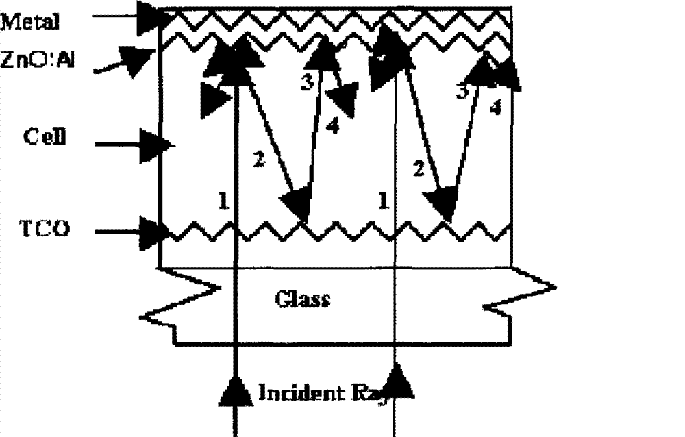
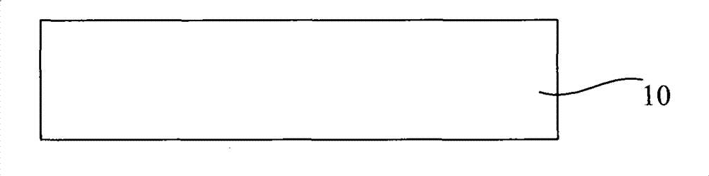
[0048] Please refer to figure 2 , providing a substrate 10, the substrate 10 may be glass, such as common Corning 1737 glass. Of course, the substrate 10 may also be made of other materials, such as other materials applicable to solar cells or flat panel display panels. Here, only the substrate 10 is made of glass as an example for illustration.

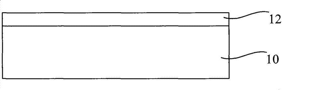
[0049] Next, please refer to image 3 , forming a seed layer 12 containing zinc oxide on the substrate 10, wherein the process of forming the seed layer 12 may be magnetron sputtering.

[0050] In the magnetron sputtering method of this embodiment, AZO (aluminum oxide content is 0.2 to 2wt.%) is used as the target material, and the aluminum in AZO is used as the impurity material of the seed layer formed, and the seed layer formed is aluminum-doped Doped zinc oxide, aluminum is used to improve electrical conductivity.

[0051] Wherein, in the process of forming the seed layer by the magnetron sputtering method of the present emb...

Embodiment 2

[0062] In this example, the processes for forming the seed layer containing zinc oxide and the main layer containing zinc oxide are metal-organic chemical vapor deposition methods, and in the deposition process, diethyl zinc (DEZ) is used as the zinc source and water vapor is used as the oxygen source. By controlling the flow rate of diethyl zinc or process temperature, etc., the growth rate and grain size of the formed zinc oxide film can be controlled. In this embodiment, the growth rate and microstructure of the zinc oxide film are adjusted by adjusting the flow rate of diethyl zinc, and the process temperature is controlled at 130°C to 160°C, specifically about 155°C. In the zinc oxide film, the with B 2 h 6 Doping boron impurities as a dopant, B 2 h 6 The doping ratio with DEZ (flux doping ratio) is about 0.6.

[0063] Wherein, in the zinc seed layer deposition process, the flow rate of diethyl zinc is 5 sccm to 10 sccm, the water vapor flow rate is 6 sccm to 13 sccm...


PUM

PropertyMeasurementUnit
thicknessaaaaaaaaaa
thicknessaaaaaaaaaa
thicknessaaaaaaaaaa

Abstract

The invention relates to a preparation method of a transparent conducting film, which is used for forming a transparent conducting film containing zinc oxide on a base and comprises the steps of forming a seed layer containing the zinc oxide on the base, and forming a main body layer containing the zinc oxide on the seed layer. The invention also provides a transparent conducting film, a display device and a solar battery. The preparation method of the invention can increase the speed rate of the formation of the transparent conducting film. The transparent conducting film of the invention has higher photoelectric conversion efficiency.

Description

technical field [0001] The invention relates to the technical field of semiconductors, in particular to a transparent conductive film and a manufacturing method thereof, a solar cell and a flat panel display device. Background technique [0002] Transparent Conductive Oxide semiconductor thin film (Transparent Conductive Oxides, TCO referred to as transparent conductive film) has been widely used in many fields due to its unique optical and electrical properties. The basic characteristics of the transparent conductive film include that the band gap is generally greater than 3eV, so it has ultraviolet cut-off characteristics; the transmittance in the visible light region is generally greater than 80%; the reflectivity in the infrared region is generally greater than 80%; it has strong attenuation for microwaves. At present, transparent conductive films are mainly used in solar cells, transparent electrodes of flat panel displays, electromagnetic protective screens, and infrar...

Claims


Application Information

Patent Timeline
Patent Type & Authority Patents(China)
IPC IPC(8): C23C28/00C23C14/35C23C16/18H01B5/14H01L21/28H01L31/18H01L51/48H01L51/56H01L31/0224H01L51/44H01L27/32H01L51/52H01L33/00G02F1/1343G06F3/042
CPCY02E10/549Y02P70/50
Inventor 徐亚伟
Owner BEIJING NAURA MICROELECTRONICS EQUIP CO LTD
Why Eureka
Try Eureka