High-voltage asymmetric structure ldmos device and its preparation method

An asymmetric structure and device technology, which is applied in semiconductor/solid-state device manufacturing, semiconductor devices, electrical components, etc., can solve the problem of increased on-resistance of devices, achieve the effects of improving breakdown voltage, ensuring performance, and improving control capabilities

Active Publication Date: 2021-03-09
BEIJING CHIP IDENTIFICATION TECH CO LTD +2
View PDF8 Cites 0 Cited by
  • Summary
  • Abstract
  • Description
  • Claims
  • Application Information

AI Technical Summary

Problems solved by technology

The design of LDMOS is mainly carried out around the reasonable compromise between the breakdown voltage and the characteristic on-resistance. Increasing the device withstand voltage by increasing the length of the drift region will lead to a sharp increase in the device on-resistance

Method used


Image

  • High-voltage asymmetric structure ldmos device and its preparation method
  • High-voltage asymmetric structure ldmos device and its preparation method
  • High-voltage asymmetric structure ldmos device and its preparation method

Examples


Embodiment 1

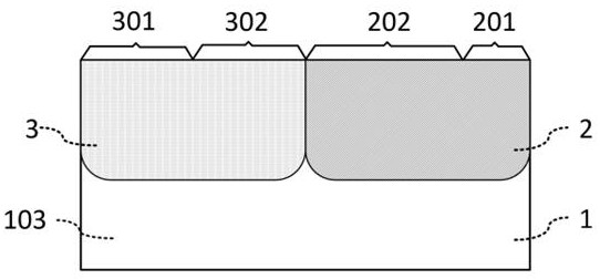
[0051] figure 1 It is a schematic structural diagram of a high-voltage asymmetric structure LDMOS device provided in the first embodiment of the present invention. In this embodiment, the drift region 2 and the body region 3 of the LDMOS device are in lateral contact.

[0052] specific reference Figure 1 to Figure 7 As shown, the LDMOS device has: a drift region 2 and a body region 3; the surface of the drift region 2 is divided into a first region 201 and a second region 202; the surface of the body region 3 is divided into a third region 301 and a The fourth region 302, the second region 202 and the fourth region 302 are extended and covered by the first gate dielectric layer 4; the surface of the first gate dielectric layer 4 is divided into a seventh region 401, the seventh region 401 is located above the drift region 2 and covered by the second gate dielectric layer 5; the surface of the second gate dielectric layer 5 is divided into a sixth region 502 and a fifth regi...

Embodiment 2

[0058] Figure 8 It is a schematic structural diagram of a high-voltage asymmetric structure LDMOS device provided by the second embodiment of the present invention. In this embodiment, the drift region 2 and the body region 3 of the LDMOS device are laterally spaced apart by the ninth region 103 of the substrate 1 .

[0059] Figure 9 It is a flow chart of a method for manufacturing a high-voltage asymmetric structure LDMOS device provided by an embodiment of the present invention, such as Figure 9 Shown, described preparation method comprises:

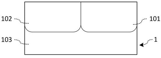
[0060] S1: dividing the eighth region 102 on the substrate to form the body region 3; dividing the tenth region 101 to form the drift region 2;

[0061] S2: Divide a first region 201 and a second region 202 on the surface of the drift region 2; divide a third region 301 and a fourth region 302 on the surface of the body region 3, the second region 202 and the The fourth area 302 is adjacent to each other;

[0062] S3: growing a...


PUM


Abstract

The invention provides a high-voltage asymmetric structure LDMOS device and a preparation method thereof. The LDMOS device includes: a drift region and a body region; the surface of the drift region is divided into a first region and a second region; the surface of the body region is divided into a third region and a fourth region, and the second region and the fourth region are divided by the first gate The dielectric layer is extended and covered; the surface of the first gate dielectric layer is divided into a seventh region, and the seventh region is located above the drift region and covered by the second gate dielectric layer; the surface of the second gate dielectric layer is divided into a sixth region and a fifth region , the first gate dielectric layer outside the fifth region and the seventh region is covered by the polysilicon gate extension; the first region of the drift region forms a drain region from the surface inward; the third region of the body region forms an active region from the surface inward , the depth of the drain region is greater than the depth of the source region. The double-layer gate dielectric structure ensures the reliability of the device under high-voltage and high-current conditions. The junction depth of the drain region is greater than the junction depth of the source region, which effectively improves the ability of the drain region to control the conductive channel.

Description

technical field [0001] The invention relates to the technical field of semiconductor integrated circuits, in particular to a high-voltage asymmetric structure LDMOS device and a preparation method of a high-voltage asymmetric structure LDMOS device. Background technique [0002] With the development of the times, power semiconductor devices have penetrated into all aspects of national economic life. In recent years, energy conservation and environmental protection have become a topic of increasing concern worldwide, and the application fields of semiconductors have also expanded from traditional industrial control, communications, computers, and consumer electronics to new fields such as new energy, smart grids, rail transit, and automotive electronics. The pursuit of power semiconductor devices is the processing of electric energy, which is required to have high withstand voltage and high current characteristics. [0003] LDMOS (Lateral Double-Diffused MOSFET), as a latera...

Claims


Application Information

Patent Timeline
Patent Type & Authority Patents(China)
IPC IPC(8): H01L29/78H01L29/08H01L29/40H01L29/423H01L21/336
CPCH01L29/7816H01L29/0865H01L29/0882H01L29/402H01L29/42368H01L29/66681
Inventor 郁文陈燕宁付振刘芳王帅鹏邓永峰
Owner BEIJING CHIP IDENTIFICATION TECH CO LTD
Why Eureka
Try Eureka