
Tin bismuth cuprum series leadless solder and preparation method thereof

A lead-free solder and copper-based technology, applied in the direction of welding equipment, welding/cutting media/materials, welding media, etc., can solve problems such as the effect of lowering the melting point of solder, doubts about reliability, and instability of the interface layer, and achieve reduction Effects of high temperature impact damage, saving Ag consumption, and good solder wettability

Active Publication Date: 2009-03-11
BEIJING COMPO ADVANCED TECH
View PDF4 Cites 40 Cited by
  • Summary
  • Abstract
  • Description
  • Claims
  • Application Information

AI Technical Summary

Problems solved by technology

However, bismuth also brings other problems, including the large change of its composition on the mechanical properties of the alloy, the problem of 'lead' pollution, the natural supply and high cost, and the instability of the interface layer. The reliability of higher temperature occasions is questioned, especially the monotectic alloy solder of Sn-Bi, due to the large melting range, it is prone to dendrite segregation and coarsening of the structure during the solidification process, and the unbalanced stress leads to easy peeling hazards , so the alloying of Sn-Bi solder and the rapid solidification of the welding process have become its development direction
[0005] Japanese patent application 2-70033 for this reason, 5-228685 and 8-132277 disclose a series of solders, yet because all contain Ag in these patent compositions, have increased the consumption of combat readiness resource Ag, have also increased the cost of solder (as everyone knows, silver Price from 1.45 yuan / g in 2001 to 3.7 yuan / g now), and the obvious electromigration characteristics of Ag limit the promotion of Ag-containing solder
A typical example: Motorola’s patented alloy SnBi57Ag1, although its strength and reliability are greatly improved compared with the Sn-Bi eutectic type, but the alloy not only contains the precious metal silver but also has a Bi content as high as 57%. The economical development direction of products; the U.S. patent 6,156,132 applied by Fuji Electronics and the newly launched Sn-35Bi-1Ag low-temperature solder also contain 1% precious metal Ag, which doubles the cost; the limited resources of Bi and the total cost of Sn-Bi The large-scale application of crystalline solder has led to rapid growth of Bi price, so low-Bi content silver-saving (or silver-free) solder is urgently needed to be developed
The Sn-Bi-Cu component (containing 0.1-2.0% Cu, 1.0-7.5% Bi) disclosed in U.S. Patent 6,180,264, although the use of Ag is excluded, its Bi content is too low to make it still high Solder with tin content, which inevitably has high tin defects: such as corrosion to containers and equipment, high energy consumption for welding and smelting, high tin slag output, etc., the most important thing is that lower Bi content will lower the melting point of solder The effect is limited, and the impact damage to electronic components is increased during brazing
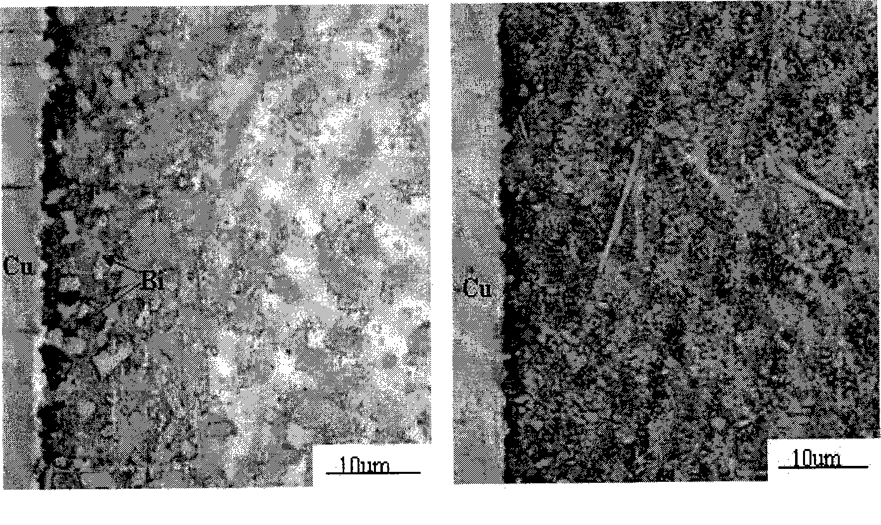
The monotectic alloy solder—silver-free Sn-Bi-Cu lead-free solder (CN200610089257.4) released by Beijing Kangpu Xiwei Solder Co., Ltd. and Beijing General Research Institute of Nonferrous Metals to a large extent suppresses the Bi element in the process of solder solidification. segregation, but it will inevitably form a weak zone of Bi-rich layer at the welding interface, resulting in poor reliability of solder joints (greater cracking tendency)

Method used


Image

  • Tin bismuth cuprum series leadless solder and preparation method thereof
  • Tin bismuth cuprum series leadless solder and preparation method thereof
  • Tin bismuth cuprum series leadless solder and preparation method thereof

Examples


Embodiment 1

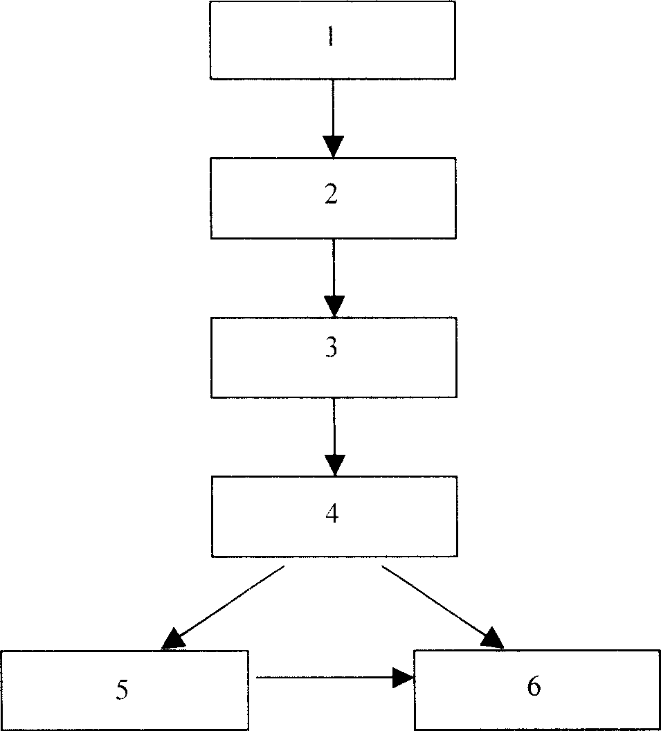
[0027] Preparation of Sn-29Bi-0.5Cu-0.1Zn alloy: Prepare 5.0 kg of Sn-Cu10 and Sn-Zn9 master alloys in a vacuum intermediate frequency induction melting furnace. Melt in a melting furnace to 650°C, add weighed pure Cu flakes or pure Zn blocks, strengthen stirring and melt to a furnace temperature of 500-600°C, stir and keep warm for 10 minutes, pour into square ingots to prepare Sn-Cu10 and Sn-Zn9 Master alloy; ② Analyze the uniformity of master alloy composition. Weigh 5g of Sn-Cu10 master alloy, 1.1g of Sn-Zn9 master alloy, 29g of pure Bi, and 64.9g of pure Sn. Then melt and heat pure Sn to 290°C in a resistance furnace, add weighed pure Bi and Sn-Cu10 master alloy in turn, and finally put Sn-Zn9 master alloy, heat to 290°C and keep it for 10 minutes, and pour it into a cylindrical mold In the process, after the ingot is completely solidified, remelt the ingot to 250 ° C for 10 minutes, pull out the surface oxide slag, and pour it into the ingot mold to make an ingot for la...

Embodiment 2

[0029] Preparation of Sn-29Bi-0.5Cu-0.05Zn-0.1Ni alloy: The preparation of the master alloy is the same as in Example 1, except that the melting temperature is 900°C when preparing the Sn-Ni10 master alloy. Weigh 5g of Sn-Cu10 master alloy, 29g of pure Bi, 0.56g of Sn-Zn9 master alloy, 1g of Sn-Ni10 master alloy, and 4.44g of pure Sn. Then melt and heat pure Sn to 290°C in a resistance furnace, add weighed pure Bi and three intermediate alloys in turn, heat to 290°C for 10 minutes, pour it into a cylindrical mold, and wait until the ingot is completely solidified before adding The ingot was remelted to 250°C for 10 minutes, the surface oxide slag was pulled out, and poured into an ingot mold to make an ingot for later use.

Embodiment 3

[0031] Preparation of Sn-29Bi-0.5Cu-0.5Zn alloy: the preparation method is the same as Example 1. Weigh 5g of Sn-Cu10 master alloy, 29g of pure Bi, 5.56g of Sn-Zn9 master alloy, and 60.44g of pure Sn. Melt pure Sn in a resistance furnace and heat it to 290°C, add weighed pure Bi and Sn-Cu10, Sn-Zn9 master alloys in turn, heat to 290°C and keep it for 10 minutes, pour it into a cylindrical mold, and wait until the ingot is completely cast After solidification, remelt the ingot to 250°C for 10 minutes, and pour it into an ingot mold to make an ingot for later use.


PUM


Abstract

The invention relates to a tin-bismuth-copper series lead-free solder and a manufacture method thereof. Counted by weight percentage, the invention is characterized by including 29 minus or plus 1 percent of Bi, 0.5 minus or plus 0.1 percent of Cu, equal to or more than 0.005 percent and equal to or less than 0.5 percent of Zn; the rest is tin. The solder has a higher reliability; the solidifying segregation of the element Bi is remarkably restrained; the tissues of the welding points are uniform and thin; no pure-Bi layers appear on a welding interface; the IMC (compound between metals) stability of the interface is improved; the interface has excellent technique property, mechanical property and using reliability. The tin-bismuth-copper series lead-free solder can be widely applied to the low-temperature encapsulation occasion and the multilevel encapsulation occasion of an electric product.

Description

technical field [0001] The invention relates to the technical field of manufacturing tin-based lead-free solder for low-temperature assembly in the electronics industry, in particular to a modified tin-bismuth-copper-based lead-free solder and a preparation method thereof. Background technique [0002] Solder is widely used in connecting materials such as electronic appliances. However, with the recognition of the toxicity of Pb and the continuous improvement of solder requirements for electronic products, lead-free solder has become the mainstream. As a new type of lead-free electronic packaging solder, the general requirements are: it should have good process performance (low melting point, good wettability, good corrosion resistance and oxidation resistance, good mechanical properties, good conductivity), high process yield (fast spreading speed, high welding yield, high slag formation rate), good reliability of solder joints (high joint strength of solder joints, good cr...

Claims


Application Information

Patent Timeline
IPC IPC(8): B23K35/26C22C1/03B22F9/08
Inventor 徐骏胡强贺会军张富文王志刚卢彩涛赵朝辉高德云
Owner BEIJING COMPO ADVANCED TECH
Learn More