Multiprocessor computing apparatus with wireless interconnect and non-volatile random access memory

a multi-processor computing and wireless interconnection technology, applied in the field of multi-processor computing apparatuses, can solve problems such as cis or mis, and achieve the effects of reducing power consumption, facilitating high throughput, and high speed

Active Publication Date: 2018-02-13
PATEL SURESHCHANDRA B
View PDF11 Cites 1 Cited by
  • Summary
  • Abstract
  • Description
  • Claims
  • Application Information

AI Technical Summary

Benefits of technology

[0034]As said before, ICs are networks / circuits in packages interconnecting thousands or millions or billions of discrete electronic components like transistors, diodes, resistors, capacitors etc. depending on level of integration such as SSI or LSI or VLSI using MIs or next-generation evolving CIs. However, integration of discrete electronic components is carried out to create various functional blocks and storage blocks / units in VLSI such as SoC, SiP, NoC etc. The best approach appears to be scaling of MIs or emerging CIs only to a point of formation of each functional block and / or storage block, and then providing Wireless Interconnect (WLI) involving TRAs for communication among various functional and / or storage blocks. That is to say, intra-functional block uses MIs or emerging CIs, and inter-functional blocks use WLIs involving TRAs. The definition of functional block can vary from designer to designer. For example, a functional block can further be divided into sub-functional blocks and providing MIs or CIs for communication within / intra sub-functional blocks and WLIs involving TRAs for communication among / inter sub-functional blocks as per FIG. 8b along with WLIs involving TRAs among / inter functional blocks. There are two extremes to this approach: at one end, there are no WLIs involving TRAs used as per current status of the interconnect technologies, and at the other ideally there are no MIs or CIs used. Hopefully, the other extreme end, wherein interconnect technology that do not use MIs or CIs at all will soon be reached. The WLIs involving TRAs technology has advantages of re-configurability, system scalability / expandability, and fault tolerance, which are not possible with fixed wire-line MIs or CIs. At the system level fault tolerance can be achieved by software commands to debug and then to eliminate the faulty chips via reconfiguration. Moreover, MIs or CIs using physical “wired” channels for data transport do not resolve the difficult problem of routing the interconnect because they involve consequent time delaying and power consuming switching operations, whereas, WLIs involving TRAs make it possible for every functional block to be able to communicate directly with all others at the speed of light, which is the highest possible. Particularly every processor of MCA can access every unit of shared memory directly with WLIs involving TRAs. Therefore, while allowing for material innovations like CNTs and GNRs for intra-functional CIs, and by using WLIs involving TRAs for inter-functional communication, the present invention attempts to overcome a brick wall by radically different interconnect architectures based on other forms of technology scaling as described in the following. While cut-off switching speed of transistors is expected to be 600 GHz for the next 16 nm technology generation, it may be possible to raise the operational clock frequency of MCAs to 10 GHz and much higher with technology scaling of the present invention along with the use of CIs for intra functional communications.
[0035]It is the primary object of the present invention to introduce wireless interconnects for communication among various components of Multiprocessor Computing Apparatus in order to dramatically reduce latency and contention for shared resources for the purpose of parallel processing. MCA comprises 2 or more processors, and sometimes of the order of thousands or millions of processors in case of massively parallel computing apparatus, each processor having local private memory (PM), and an access to shared memory divided into SMUs, and also access to other shared resources including I / Os devices.
[0037]The WLI comprises Transmitter-Receiver-Antenna (Transceiver-Antenna:TRA) mounted / fabricated / -integrated / embedded on each of the multiprocessors and shared resources, and electromagnetically shielded and sealed confined free space within Metallic Enclosure (ME) housing MCA. The ME is made up of pure or alloyed metal that is very good conductor of both heat and electricity. The invention is in general about wireless communication within electromagnetically shielded and sealed confined free space that is part of any apparatus, equipment, or device including MCA. WLI can use the whole range of frequencies that can be generated by oscillators of transceivers for transmitting and receiving information to achieve communication among components of MCA. The whole range of frequencies involves the range from lows of 10s HZs to highs of GHZs and beyond. The use of WLI involving TRA makes it possible for each Processing Unit (PU) of MCA to be able to address large number of SMUs because an address for each of SMUs is the frequency to which its transceiver is permanently tuned to send and receive information / data. A significant achievement of this invention is that each processor of MCA is capable of addressing almost unlimited shared memory. The smallest SMU could be consisting of a single addressable memory location. That means in a best possible scenario each processor of MCA can reach and communicate with every single addressable memory location directly.
[0039]The invented WLI involving TRAs provides all-to-all direct communication links between components of MCA regardless of their topological distances. Without packet / circuit switching, WLI involving TRAs eliminates intermediate routing and buffering delays and makes signal propagation delay approach the ultimate lower bound: the speed of light. WLI involving TRAs links can operate at much higher speed than core logic making it easy to provide high throughput. In WLI involving TRAs, line of sight communication channels are built directly between communicating nodes within a network in a total distributed fashion without arbitration. An important consequence is that packets destined for the same receiver will collide. Such collisions require detection, retransmission, and extra bandwidth margin to prevent them from becoming a significant issue. The WLI involving TRAs allows errors and collusions to be handled by the same mechanism essentially requiring no extra support than needed to handle errors, which is necessary in any system.
[0040]It is also, the primary object of the present invention to introduce Universal Computer Memory for information storage and retrieval. The Universal Computer Memories are Static Magneto-Optical (SMO) and Static Optical (SO) memories that can be accessed in the same manner as currently used semiconductor Random Access Memories (RAMs). The SMO and SO RAMs are Non-Volatile Random Access Memories (NVRAMs), cheap, and consume much less power than semiconductor RAMs. Universal Computer Memory can also be made up of any media that can be written to and read from using laser (optical) read / write mechanism without requiring rotational or any other motion. It is called Universal Computer Memory in the sense that it can be used to make main computer memory similar to semiconductor RAM, and it can also be used to make bulk storage devices like hard drives.

Problems solved by technology

Moreover, MIs or CIs using physical “wired” channels for data transport do not resolve the difficult problem of routing the interconnect because they involve consequent time delaying and power consuming switching operations, whereas, WLIs involving TRAs make it possible for every functional block to be able to communicate directly with all others at the speed of light, which is the highest possible.

Method used


Image

  • Multiprocessor computing apparatus with wireless interconnect and non-volatile random access memory
  • Multiprocessor computing apparatus with wireless interconnect and non-volatile random access memory
  • Multiprocessor computing apparatus with wireless interconnect and non-volatile random access memory

Examples


Embodiment Construction

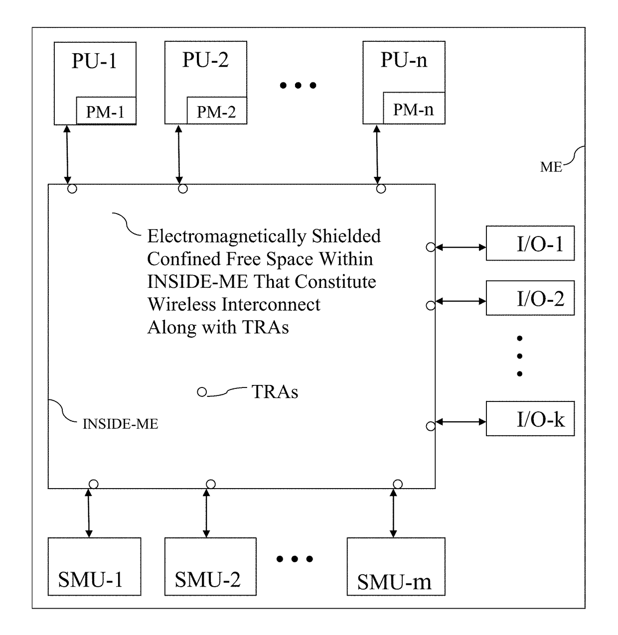
[0076]Present invention is about putting MCA or any other similar apparatus / equipment / device into an electro-magnetically shielded and sealed Metallic Enclosure (ME) or Container, and using wireless means for communication among its components mounted / fabricated / integrated / embedded with TRAs. The Wireless Interconnect (WLI) constitutes enclosed free space within an electromagnetically shielded and sealed ME and / or INSIDE-ME and TRAs mounted / fabricated / integrated / embedded one on each of the components of MCA. WLI provides a means of wireless communication among components of MCA. Aluminium, Copper, CNT, GNR or any pure or alloy metal that is good conductor of both heat and electricity can be used in making ME and INSIDE-ME. The ME also acts as heat sink for component ICs of the MCA, or an apparatus or an equipment, or a device, and if required it can be corrugated and / or finned on the outside to increase surface area for heat dissipation. The ME of MCA, or an apparatus or an equipmen...


PUM

PropertyMeasurementUnit
frequencyaaaaaaaaaa
frequencyaaaaaaaaaa
surface areaaaaaaaaaaa

Abstract

A fan-less Multiprocessor-Computing-Apparatus (MCA) housed in a Metallic-Enclosure (ME) acting as an electromagnetic-Shield for wireless-communications / interconnects (WLI) among components of MCA enabling the whole-range-frequencies from lows of 10-HZs to highs of GHZ and beyond to be able to address almost unlimited Shared-Memory-Units (SMUs) by each processor with each SMU permanently tuned to send / receive data at a particular frequency. The ME is dust-proofed and filled with clean-air / vacuum for efficient-and-reliable WLI. The ME also acts as a heat-sink with the components of MCA placed on Circuit-Boards are mounted on inside in a plane parallel to the respective side of the ME of any required size and shape and heat producing components are firmly attached to the ME, which is waterproofed and placed-under-water for cooling. The SMUs are made up of static non-volatile Random Access Memory that can be read-from and written-to optically.

Description

TECHNICAL FIELD[0001]The present invention relates to a Multiprocessor Computing Apparatus (MCA) comprising each of the multiprocessors referred to as Processing Units (PUs), each of shared resources such as Shared Memory Units (SMUs), interface circuits of peripheral components and inputs / outputs (I / Os), and wireless interconnect (WLI) for communication among PUs and shared resources that are components of MCA. Specifically, the invention relates to two components of MCA that are SMUs and WLI.BACKGROUND OF THE INVENTION[0002]Switching speed of transistors and diodes improve over each technology generation of shrinking geometries and increasing integration density or scaling of Complementary-Metal-Oxide-Semiconductor (CMOS) Integrated Circuits (ICs). As per International Technology Roadmap for Semiconductor (ITRS) for the year 2010, the cut-off frequency of switching is expected to be of the order of 600 GHZs in 16 nm CMOS technology leading to the availability of hundreds of GHZs b...

Claims


Application Information

Patent Timeline
Patent Type & Authority Patents(United States)
IPC IPC(8): G06F3/06G06F1/18G06F1/20H05K9/00G11B13/04G06F1/16G06F13/10G06F13/16G06F13/40G11B5/09H05K7/20
CPCG06F3/0604H05K9/002G06F1/1613G06F1/1656G06F1/182G06F1/20G06F3/067G06F3/0629G06F13/102G06F13/16G06F13/4068G11B5/09G11B13/045H05K7/20409G06F1/16
Inventor PATEL, SURESHCHANDRA B.
Owner PATEL SURESHCHANDRA B
Why Eureka
Try Eureka