
Ion beam processing apparatus

a technology of ion beams and processing apparatuses, applied in the field of ion beam processing apparatuses, can solve the problems of reducing the crystal structure at the depth of the crystal structure, wasting silicon materials, and limited methods in terms of how thin slices can be cu

Inactive Publication Date: 2012-01-03
VAXIS TECH
View PDF30 Cites 11 Cited by
  • Summary
  • Abstract
  • Description
  • Claims
  • Application Information

AI Technical Summary

Benefits of technology

"The present invention is about a method and apparatus for ion-slicing in semiconductor manufacturing. The invention includes two main process carousels, one for exposing workpieces to an ion beam and cooling them, and another for post-implant process steps like annealing and bonding. The first carousel supports multiple workpieces and moves them sequentially through the ion beam, while the second carousel supports multiple workpieces and performs post-implant process steps in parallel on them. The invention also includes a vacuum chamber and a load lock device for transferring workpieces in and out of vacuum. The technical effects of the invention include improved efficiency and productivity in semiconductor manufacturing."

Problems solved by technology

This method is limited in terms of how thinly the slices can be cut.
It also results in considerable waste of silicon material due to the kerf that is removed by the saw.
The resulting subsurface damage layer is concentrated around the depth where the ions stop and it weakens the crystal structure at that depth.
Subsequent external heating of the substrate consolidates the implanted gas and nucleates and grows micro-bubbles, further weakening the crystal lattice.
One technical hurdle is the removal of heat deposited by the ion beam.
On one hand, it is necessary that the implant be performed at temperatures below roughly 400 or 500 C, otherwise the implanted ions may diffuse away during implantation, or uncontrolled, premature cleaving and bubble formation could occur.
It will be readily apparent to those familiar with accelerator and ion implantation art that a further complication arises due to the necessity to produce, transport and deliver ion beams in vacuum.
Cooling of objects in vacuum is widely known to be quite difficult since there is substantially no gas present to aid in the conduction of heat across mechanical joints.
Furthermore, for relatively thick workpieces as in the solar application described above, there is an additional temperature drop between the surface receiving the ion beam treatment and the cooled back surface due to the thermal resistance of the workpiece itself.
This can negatively impact the reproducibility of the process and the size of the process window.
This is an effective method but it incurs the difficulties of processing multiple workpieces simultaneously.
The ion beam optical elements, such as electromagnets or electrostatic deflectors, which are used to scan and collimate the beam must be larger and more expensive.
All the vacuum chambers and workpiece handling mechanisms will also be larger, more complex, and more expensive in order to handle arrays of workpieces.
Such difficulties with workpiece temperature control and ion beam heating of the substrate are widely known in the ion-implantation of wafers for semiconductor chip making The problem is obviously most acute for implantation at relatively high beam current and high energy.
This approach however also requires the wafers to be processed in batches which complicates and adds cost to the equipment overall.
The large disk has significant inertia and takes time to achieve the required speed before the ion beam can be applied to the workpieces, reducing equipment productivity.

Method used


Image

  • Ion beam processing apparatus
  • Ion beam processing apparatus
  • Ion beam processing apparatus

Examples


Embodiment Construction

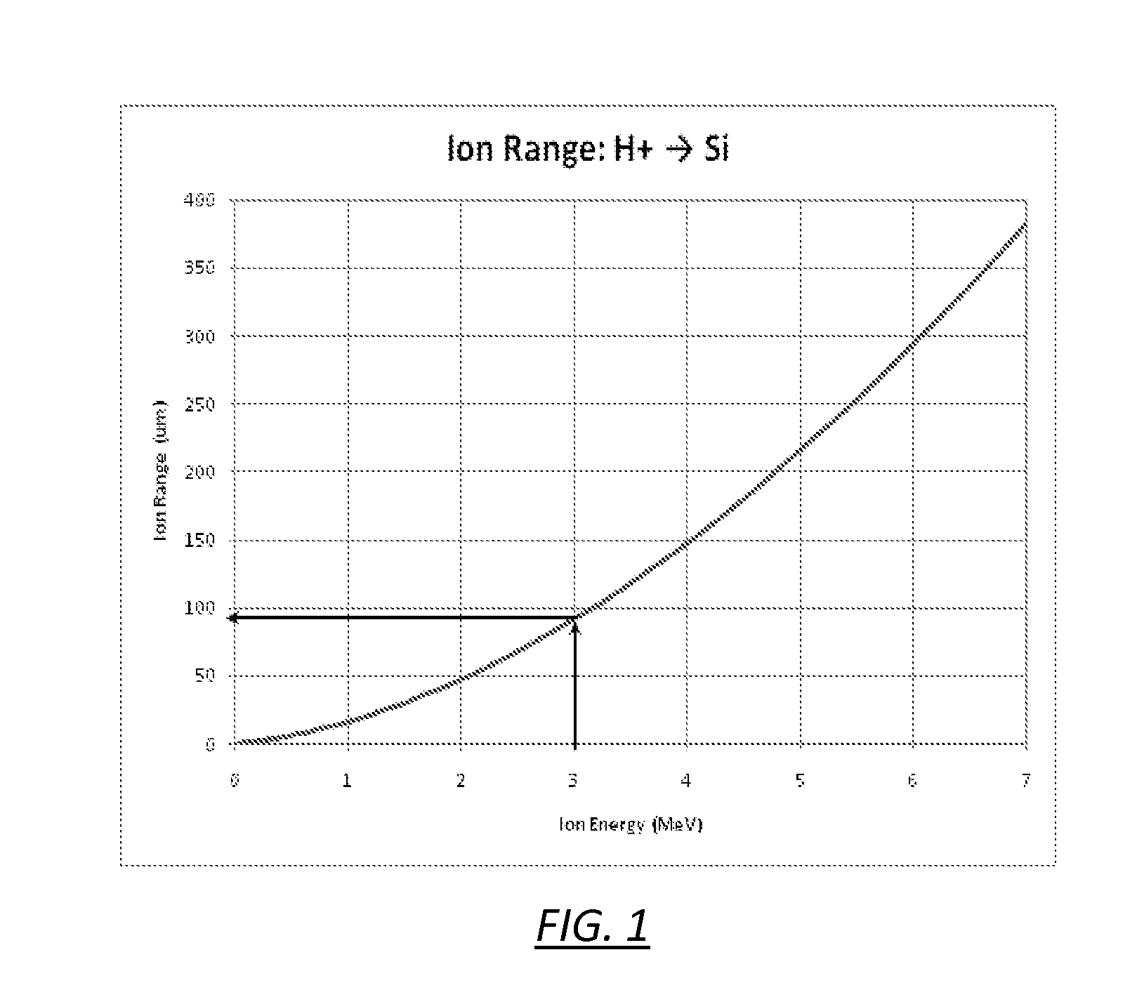
[0046]As discussed in the background section, FIG. 1 shows, for reference, a plot of the range of hydrogen ions in silicon as a function of ion energy. It is plotted from values produced by the publicly available ion simulation software SRIM.

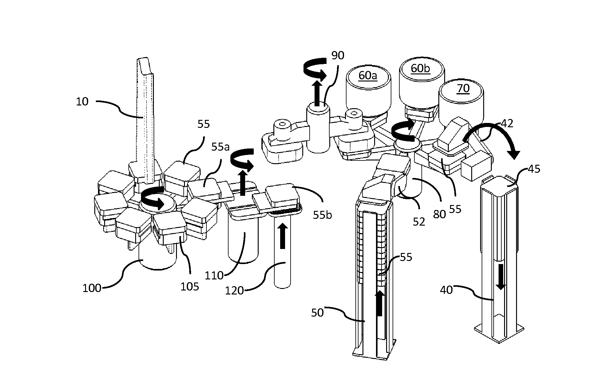
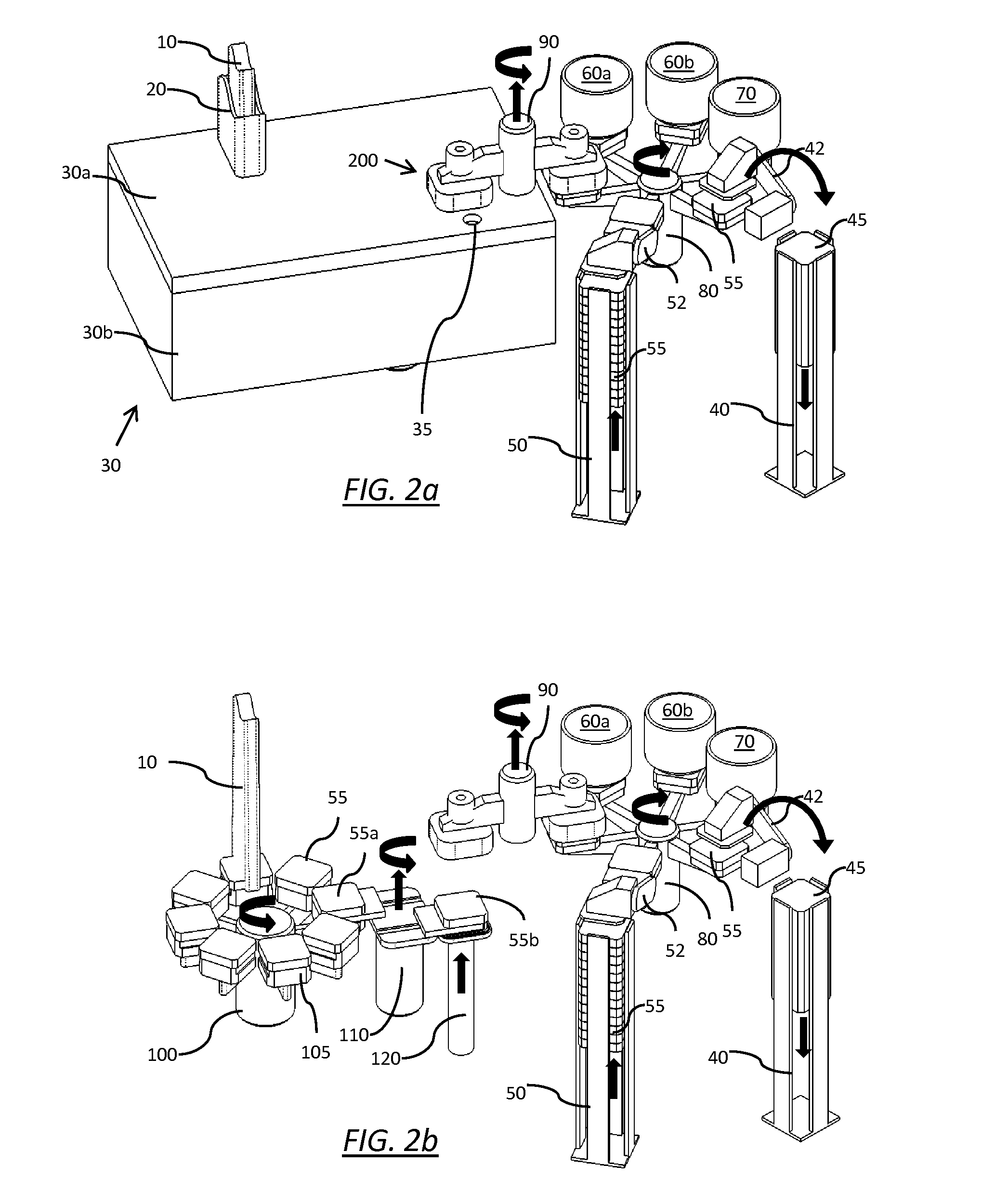
[0047]FIGS. 2a and 2b show one preferred embodiment of the ion-cut processing system. FIGS. 2a and 2b are identical except FIG. 2b has the vacuum chamber hidden to show the internal elements. In these figures some elements and details such as support structures are not shown or are simplified for clarity. Referring to FIG. 2a, ion beam 10 enters the target vacuum chamber 30 via beam tube 20 which is coupled to an ion source, accelerator, and beam delivery and scanning optics (not shown), all of which are generally under vacuum. The target vacuum chamber 30 comprises a vacuum chamber cover 30a and vacuum chamber base 30b.

[0048]Referring now to FIG. 2b, with the target vacuum chamber 30 hidden to expose the internal features, a plurality of workp...


PUM


Abstract

An ion-cut machine and method for slicing silicon ingots into thin wafers for solar cell manufacturing is set forth, amongst other embodiments and applications. One embodiment comprises two carousels: first carousel (100) adapted for circulating workpieces (55) under ion beam (10) inside target vacuum chamber (30) while second carousel (80) is adapted for carrying implanted workpieces through a sequence of process stations that may include annealing (60), cleaving (70), slice output (42), ingot replacement (52), handle bonding, cleaning, etching and others. Workpieces are essentially swapped between carousels. In one embodiment, the swapping system comprises a high throughput load lock (200) disposed in the wall of the vacuum chamber (30), a vacuum swapper (110) swapping workpieces between first carousel (100) and load lock (200), and an atmospheric swapper (90) swapping workpieces between load lock (200) and second carousel (80).

Description

CROSS-REFERENCE TO RELATED APPLICATIONS[0001]This application claims the benefit of provisional patent application No. 61 / 026,371 filed 5 Feb. 2008 by the present inventor.FEDERALLY SPONSORED RESEARCH[0002]Not applicableSEQUENCE LISTING OR PROGRAM[0003]Not applicableFIELD OF THE INVENTION[0004]This invention relates generally to equipment, techniques, and processes for ion beam-slicing of wafers and ingots of semiconductor materials and other materials. The invention is applicable to a variety of widely used processes such as ion beam induced exfoliation, ion-slicing, layer transfer, and similar processes wherein materials or workpieces are treated with or exposed to ion fluxes allowing a relatively thin layer of the material to be cleaved off and optionally bonded to another substrate. The present invention is also applicable to ion-implantation equipment used in the doping of semiconductors.BACKGROUND OF THE INVENTIONIon-Cut Process[0005]One process of interest here is the ion-cut...

Claims


Application Information

Patent Timeline
Patent Type & Authority Patents(United States)
IPC IPC(8): A61N5/00
CPCH01L21/67201H01L21/67213H01J2237/2007H01J2237/202H01J2237/204H01J2237/31701
Inventor BRAILOVE, ADAM ALEXANDER
Owner VAXIS TECH
Learn More