
Method for producing III group element nitride crystal, production apparatus for use therein, and semiconductor element produced thereby

a technology of nitride crystals and group elements, which is applied in the direction of crystal growth process polycrystalline material growth, etc., can solve the problems of inability to meet the requirements of the product quality, etc., to achieve the effect of reducing the length of time required for crystals of a desired size, reducing the length of time required for supersaturation, and reducing the time required for substantial crystal growth

Inactive Publication Date: 2010-09-14
PANASONIC CORP +1
View PDF26 Cites 0 Cited by
  • Summary
  • Abstract
  • Description
  • Claims
  • Application Information

AI Technical Summary

Benefits of technology

"The present invention provides a method for producing high-quality Group-III-element nitride crystals with improved growth rates. This is achieved through a material preparation process where nitrogen is allowed to dissolve in a melt containing the Group III element and the at least one of alkali metal and alkaline-earth metal, followed by pressurizing and heating under an atmosphere of a nitrogen-containing gas to grow crystals. The method also includes a producing apparatus with a heater, pressurizer, nitrogen-containing gas supplying means, crystal growth vessel, material preparation vessel, and material conveying means. The resulting crystals have improved quality and can be obtained in a short time."

Problems solved by technology

GaN crystals obtained in this manner generally have a dislocation density of 108 cm−2 to 109 cm−2 and thus are of inferior quality.
This method, however, includes complicated processes and thus is disadvantageous.

Method used


Image

  • Method for producing III group element nitride crystal, production apparatus for use therein, and semiconductor element produced thereby
  • Method for producing III group element nitride crystal, production apparatus for use therein, and semiconductor element produced thereby
  • Method for producing III group element nitride crystal, production apparatus for use therein, and semiconductor element produced thereby

Examples


embodiment 1

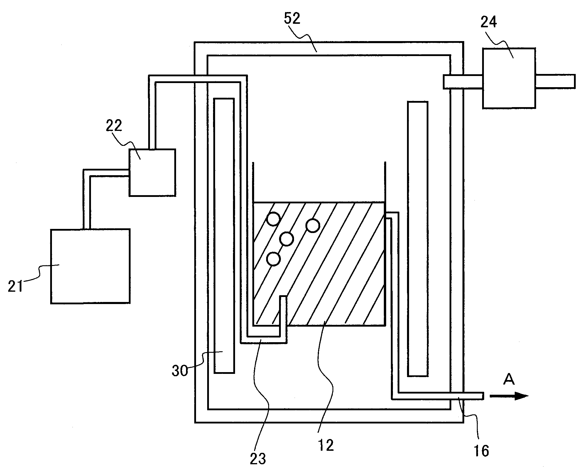
[0095]In this embodiment, GaN crystals are grown using Ga as a Group III element, a metal Na as alkali metal, and nitrogen (N2) gas as a nitrogen-containing gas. The description is directed to a method for growing the GaN crystals with reference to FIG. 7. FIG. 7 is a structural view showing an example of a configuration of an apparatus used in the producing method according to the present invention. As shown in the figure, this apparatus includes a pressure vessel 51, a gas supplying device 21, a flow amount adjuster 22, and a pressure adjuster 24 as main components. A reaction vessel 11 can be housed in the pressure vessel 51, and a heater 30 is disposed on a side face of the reaction vessel 11. The flow amount adjuster 22 and the pressure adjuster 24 are connected to the pressure vessel 51 via pipes, respectively, and the gas supplying device 21 is connected to the other end of the flow amount adjuster 22 via a pipe.

[0096]First, Ga and Na are put in the reaction vessel 11. Then, ...

embodiment 2

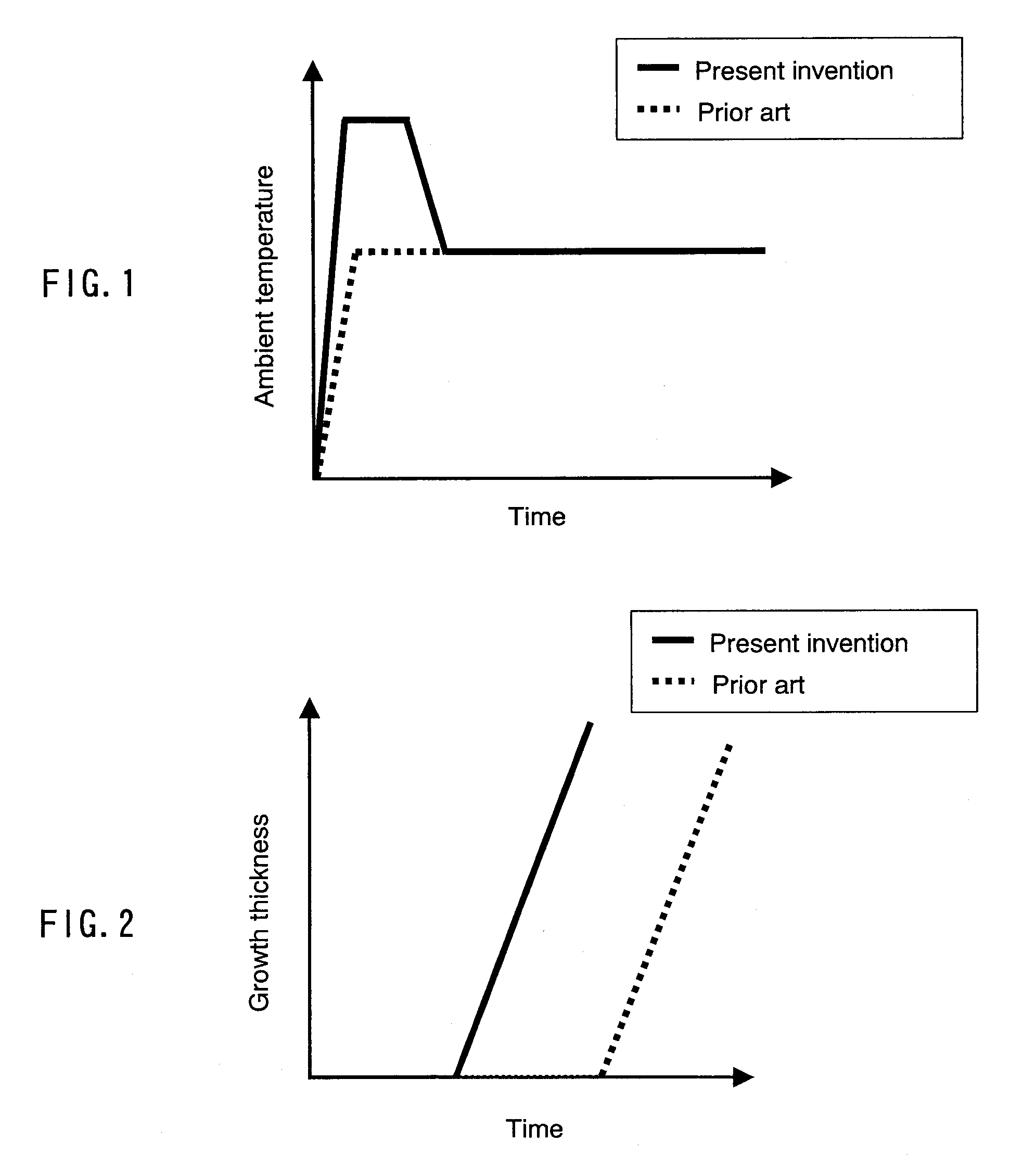
[0097]In this embodiment, GaN crystals are grown using Ga as a Group III element, a metal Na as an alkali metal, and nitrogen (N2) gas as a nitrogen-containing gas. First, an ambient pressure and an ambient temperature are set to 60 atm to 70 atm (60×1.013×105 Pa to 70×1.013×105 Pa)(a pressure higher than an ambient pressure used during a time of crystal growth by, for example, 20 atm to 30 atm (20×1.013×105 Pa to 30×1.013×105 Pa)) and 850° C., respectively, and are kept for 1 hour to 5 hours so that nitrogen is allowed to dissolve rapidly in a melt containing Ga and Na to attain a desired nitrogen concentration in the melt (material preparation process). Then, in a state where the ambient temperature is kept at 850° C., the ambient pressure is lowered to 40 atm (40×1.013×105 Pa) so that GaN crystals are grown in the melt (crystal growth process). As a result, a length of time from a start of material heating to a start of crystal growth is reduced considerably to, for example, 10 h...

embodiment 3

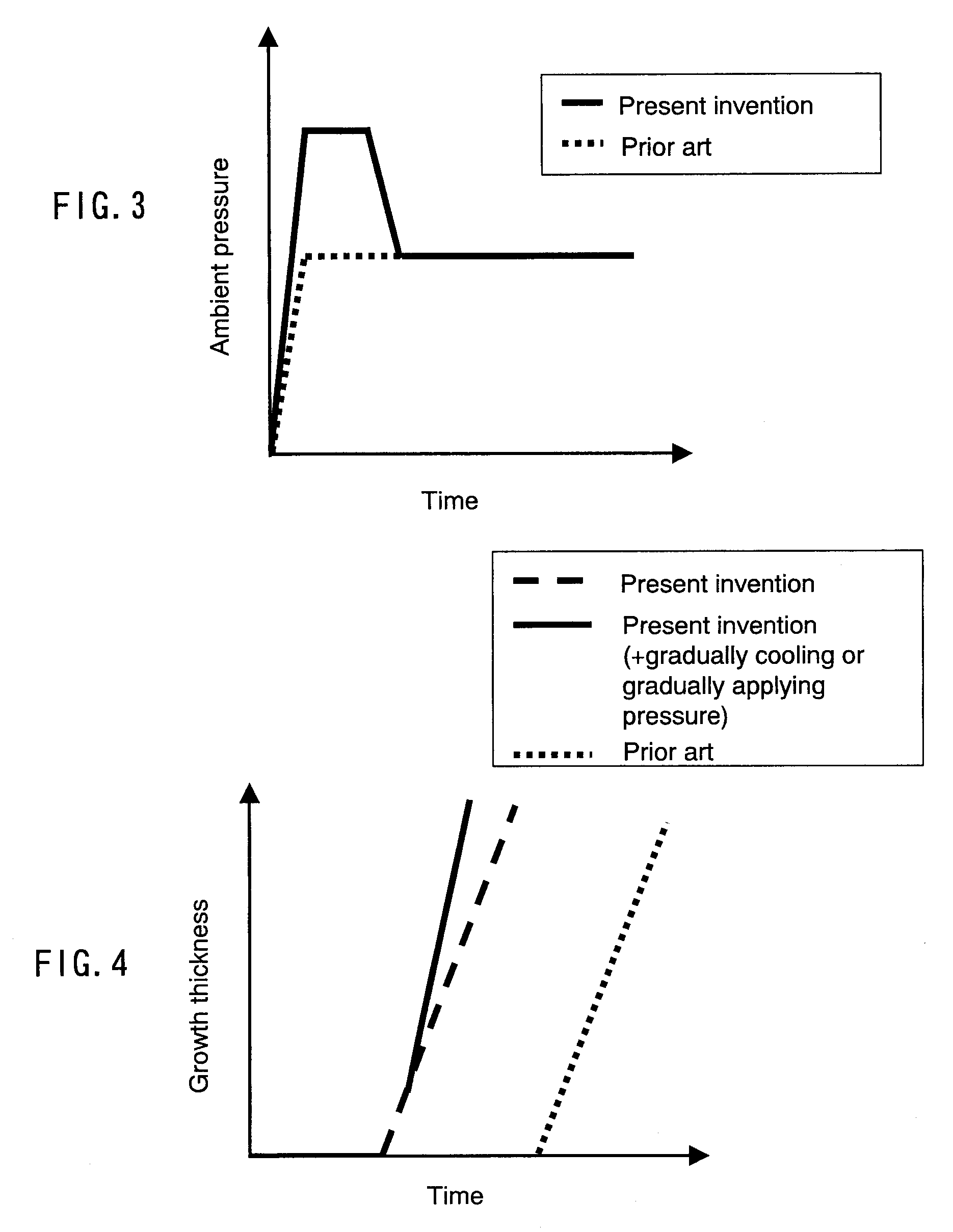
[0098]In this embodiment, first, a material preparation process is performed in the same manner as in Embodiment 1, and an ambient temperature is lowered. Then, in a crystal growth process, the ambient temperature further is lowered at a rate of 0.2° C. per hour to 1.5° C. per hour. As a result, a substantial crystal growth rate further is increased and can be, for example, 25 μm per hour. FIG. 5 shows an example of a change over time in ambient temperature in this embodiment, and FIG. 4 shows an example of a relationship between growth thickness and time in this embodiment. FIG. 4 also shows a relationship between growth thickness and time in the case where crystals are grown by the conventional method. An ambient temperature is not particularly required to be lowered linearly with respect to time and may be lowered in a step-wise manner. Further, an ambient temperature may be lowered at a rate gradually increasing in a range of, for example, 0.1° C. per hour to 1.5° C. per hour.


PUM

PropertyMeasurementUnit
pressureaaaaaaaaaa
pressureaaaaaaaaaa
temperatureaaaaaaaaaa

Abstract

A method for producing Group-III-element nitride crystals by which an improved growth rate is obtained and large high-quality crystals can be grown in a short time, a producing apparatus used therein, and a semiconductor element obtained using the method and the apparatus are provided. The method is a method for producing Group-III-element nitride crystals that includes a crystal growth process of subjecting a material solution containing a Group III element, nitrogen, and at least one of alkali metal and alkaline-earth metal to pressurizing and heating under an atmosphere of a nitrogen-containing gas so that the nitrogen and the Group III element in the material solution react with each other to grow crystals. The method further includes, prior to the crystal growth process, a material preparation process of preparing the material solution in a manner that under an atmosphere of a nitrogen-containing gas, at least one of an ambient temperature and an ambient pressure is set so as to be higher than is set as a condition for the crystal growth process so that the nitrogen is allowed to dissolve in a melt containing the Group III element and the at least one of alkali metal and alkaline-earth metal. The method according to the present invention can be performed by using, for example, the producing apparatus shown in FIG. 7.

Description

CROSS-REFERENCE RELATED APPLICATIONS[0001]This application is a National Stage Entry of PCT / JP05 / 06365 filed Mar. 31, 2005.TECHNICAL FIELD[0002]The present invention relates to a method for producing Group-III-element nitride crystals, a producing apparatus used therein, and a semiconductor element obtained using the method and the apparatus.BACKGROUND ART[0003]Attention has been drawn to gallium nitride (GaN) as a material for semiconductor elements that emit blue or ultraviolet light. A laser diode (LD) that emits blue light is used for high-density optical disks and displays, and a light-emitting diode (LED) that emits blue light is used for displays, lighting and the like. Further, an ultraviolet LD is expected to be used in the field of biotechnology or the like, and an ultraviolet LED is expected to be used in fluorescent lamps to emit ultraviolet light.[0004]Generally, GaN crystals that are used for LDs or LEDs are formed by heteroepitaxially growing GaN crystals on a sapphir...

Claims


Application Information

Patent Timeline
Patent Type & Authority Patents(United States)
IPC IPC(8): C30B9/00C30B30/04C30B28/06C30B11/00C30B9/08C30B9/10C30B29/38
CPCC30B9/10C30B29/403C30B29/406Y10T117/1096Y10T117/1092
Inventor MINEMOTO, HISASHIKITAOKA, YASUOKIDOGUCHI, ISAOMORI, YUSUKEKAWAMURA, FUMIOSASAKI, TAKATOMOTAKAHASHI, YASUHITO
Owner PANASONIC CORP
Learn More