
Polycrystalline silicon producing method

a polycrystalline silicon and production method technology, applied in the direction of silicon compounds, electric/magnetic/electromagnetic heating, transportation and packaging, etc., can solve the problems of excessive supply of raw material gas, decrease of polycrystalline silicon yield per amount of raw material supply, etc., to prevent meltdown of rods and grow in a short time

Active Publication Date: 2013-08-13
HIGH-PURITY SILICON CORP
View PDF23 Cites 0 Cited by
  • Summary
  • Abstract
  • Description
  • Claims
  • Application Information

AI Technical Summary

Benefits of technology

The present invention is a method for producing polycrystalline silicon. The method involves controlling the pressure and amount of raw material gas supplied in two steps to prevent meltdown and produce a smooth-surfaced, round bar-shaped rod suitable for semiconductors. By supplying a larger amount of raw material gas at higher pressure in the first step, the rod can be grown in a short time. In the second step, the current and raw material gas supply are controlled to maintain the temperature of the rod center at a predetermined range to prevent meltdown, resulting in a large-diameter polycrystalline silicon rod in the shortest time and with a high level of polycrystalline silicon deposition per unit of chlorosilanes supply.

Problems solved by technology

On the other hand, it is not preferable that raw material gas is excessively supplied because a ratio of the raw material gas contributing to the deposition reaction of polycrystalline silicon decreases, and thus a deposition amount of polycrystalline silicon per an amount of raw material supply (yield of the polycrystalline silicon) decreases.

Method used


Image

  • Polycrystalline silicon producing method
  • Polycrystalline silicon producing method
  • Polycrystalline silicon producing method

Examples


examples

[0102]Next, specific examples will be described.

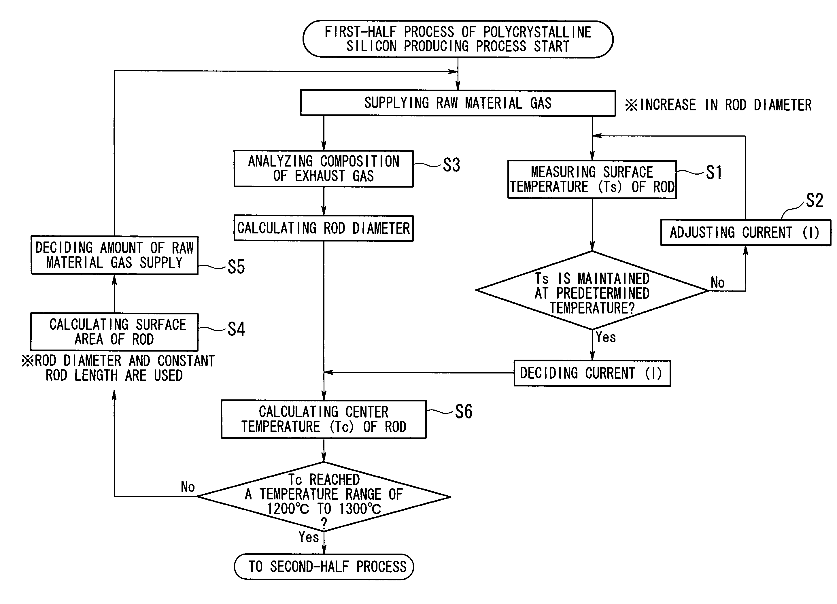
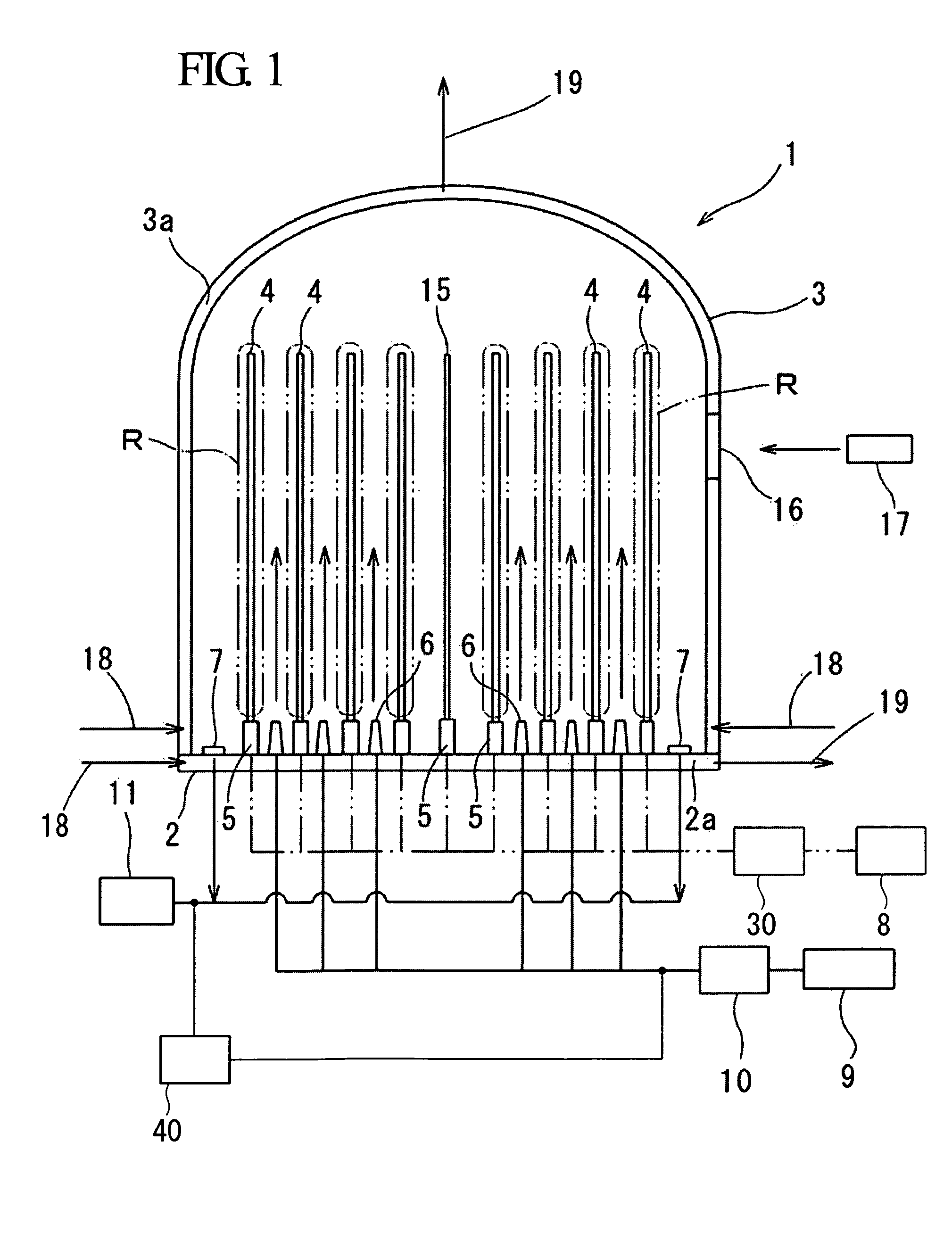
[0103]In the following examples of the polycrystalline silicon producing process, a reactor was supplied with raw material gas, in which chlorosilanes including trichlorosilane as a main component and 4.5 mol % of dichlorosilane (SiH2Cl2) were used and mixed with hydrogen (H2), so as to have a molar ratio of H2 / chlorosilanes of 8. A pressure and a supply amount of chlorosilanes per square millimeter of the surface of the rod were set as shown in Tables 1 and 2 and a current value was adjusted so that a surface temperature Ts of the rod was 1100° C. Table 1 shows examples and Table 2 shows comparative examples. The temperature of the supplying raw material gas was adjusted to 100° C. and the temperature of an inner surface of the reactor was adjusted to 200° C.

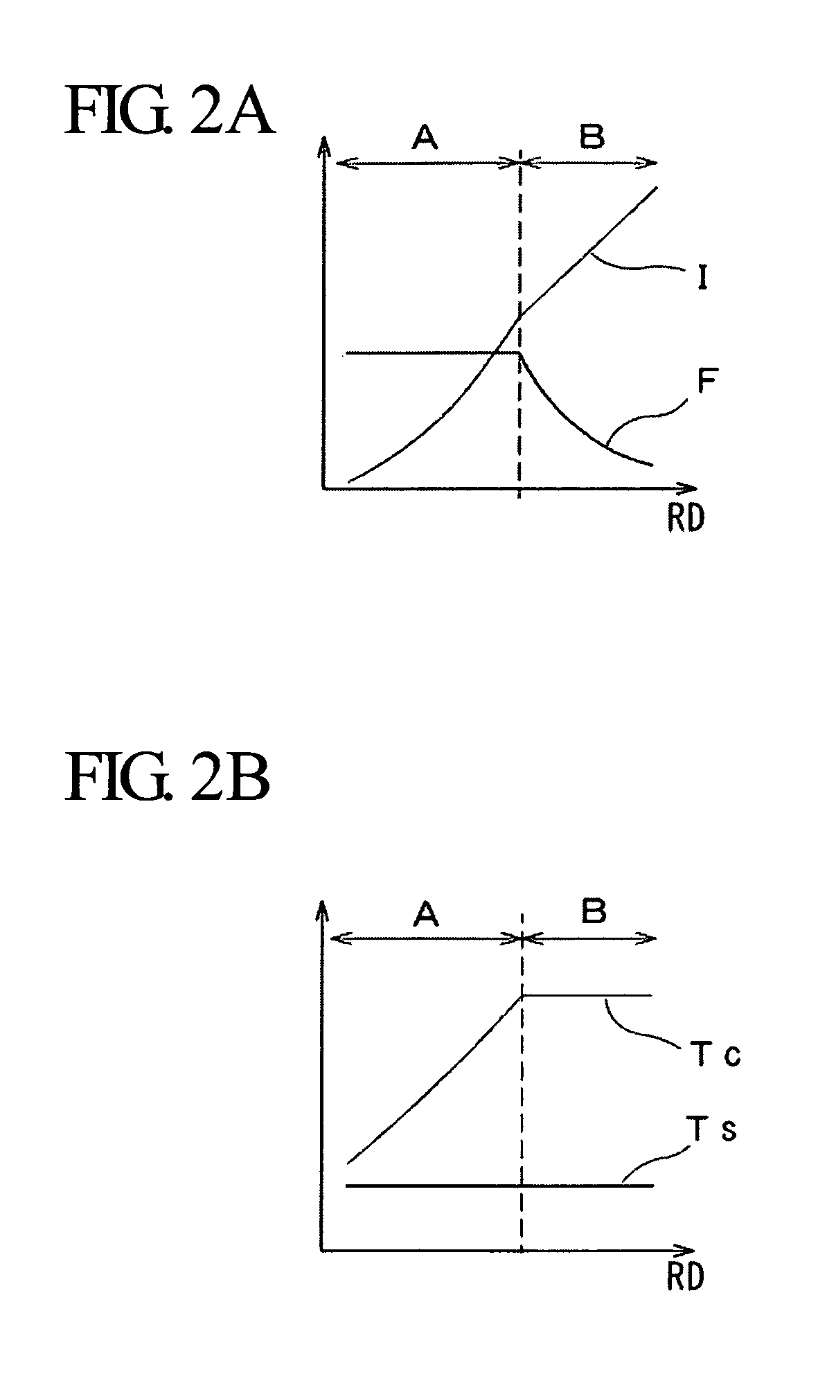
[0104]In the comparative examples, as shown in FIG. 10A, a supply amount F of chlorosilanes per square millimeter of the surface of the rod was constant and a current value I was ...


PUM

PropertyMeasurementUnit
pressureaaaaaaaaaa
pressureaaaaaaaaaa
temperatureaaaaaaaaaa

Abstract

A polycrystalline silicon producing method includes: the first process and the second process. In the first process, a surface temperature is maintained at a predetermined range by adjusting the current value to the silicon seed rod, and the raw material gas is supplied while maintaining a supply amount of chlorosilanes per square millimeter of the surface of the rod in a predetermined range until a temperature of the center portion of the rod reaches a predetermined temperature lower than the melting point of the polycrystalline silicon, and in the second process, a previously determined current value is set corresponding to a rod diameter and the supply amount of the raw material gas per square millimeter of the surface of the rod is decreased to maintain the surface temperature and the temperature of the center portion of the rod at predetermined ranges, respectively.

Description

BACKGROUND OF THE INVENTION[0001]1. Field of the Invention[0002]The present invention relates to a polycrystalline silicon producing method, an apparatus for producing the polycrystalline silicon, and the polycrystalline silicon produced by the polycrystalline silicon producing method.[0003]Priority is claimed on Japanese Patent Application No. 2009-167185, filed Jul. 15, 2009, the content of which is incorporated herein by reference.[0004]2. Description of Related Art[0005]As a polycrystalline silicon producing method, a method of producing by the Siemens method has been known. According to this polycrystalline silicon producing method, a plurality of silicon seed rods stand upright in a reactor and are supplied electric current and heated, and raw material gas including chlorosilane gas and hydrogen gas is supplied to the reactor to bring the raw material gas into contact with the heated silicon seed rods. On the surface of the heated silicon seed rods, polycrystalline silicon is ...

Claims


Application Information

Patent Timeline
Patent Type & Authority Patents(United States)
IPC IPC(8): C23C16/24
CPCC01B33/035C01B33/02C23C16/46C23C16/24Y10T428/2975Y10T428/12
Inventor URUSHIHARA, MAKOTOMIZUSHIMA, KAZUKI
Owner HIGH-PURITY SILICON CORP
Learn More