
Method of manufacturing semiconductor devices

a manufacturing method and semiconductor technology, applied in semiconductor devices, semiconductor/solid-state device details, electrical devices, etc., can solve the problems of difficult to solve the above two problems at the same time, and achieve the effect of preventing plating growth which causes a short between sub-lines, reducing production costs, and reducing production costs

Inactive Publication Date: 2011-03-22
LAPIS SEMICON CO LTD
View PDF3 Cites 0 Cited by
  • Summary
  • Abstract
  • Description
  • Claims
  • Application Information

AI Technical Summary

Benefits of technology

The present invention provides a semiconductor device manufacturing method that can prevent shorts between lines in semiconductor devices and improve yield and reliability. The method includes steps of forming connection pads on a substrate, adding an insulating film and protective film to expose the connection pads, forming sub-lines to fill the connection pad exposing holes, adding a coating film to cover the sub-lines and protective film, adding external connection electrodes, and adding a sealing layer. The method also prevents electromigration and shorts between sub-lines after sealing. The method results in a semiconductor device with improved yield and reliability.

Problems solved by technology

However, the techniques disclosed in References 1 and 2 deal with only either of the above two problems, and it was difficult to solve the above two problems at the same time.

Method used


Image

  • Method of manufacturing semiconductor devices
  • Method of manufacturing semiconductor devices
  • Method of manufacturing semiconductor devices

Examples


Embodiment Construction

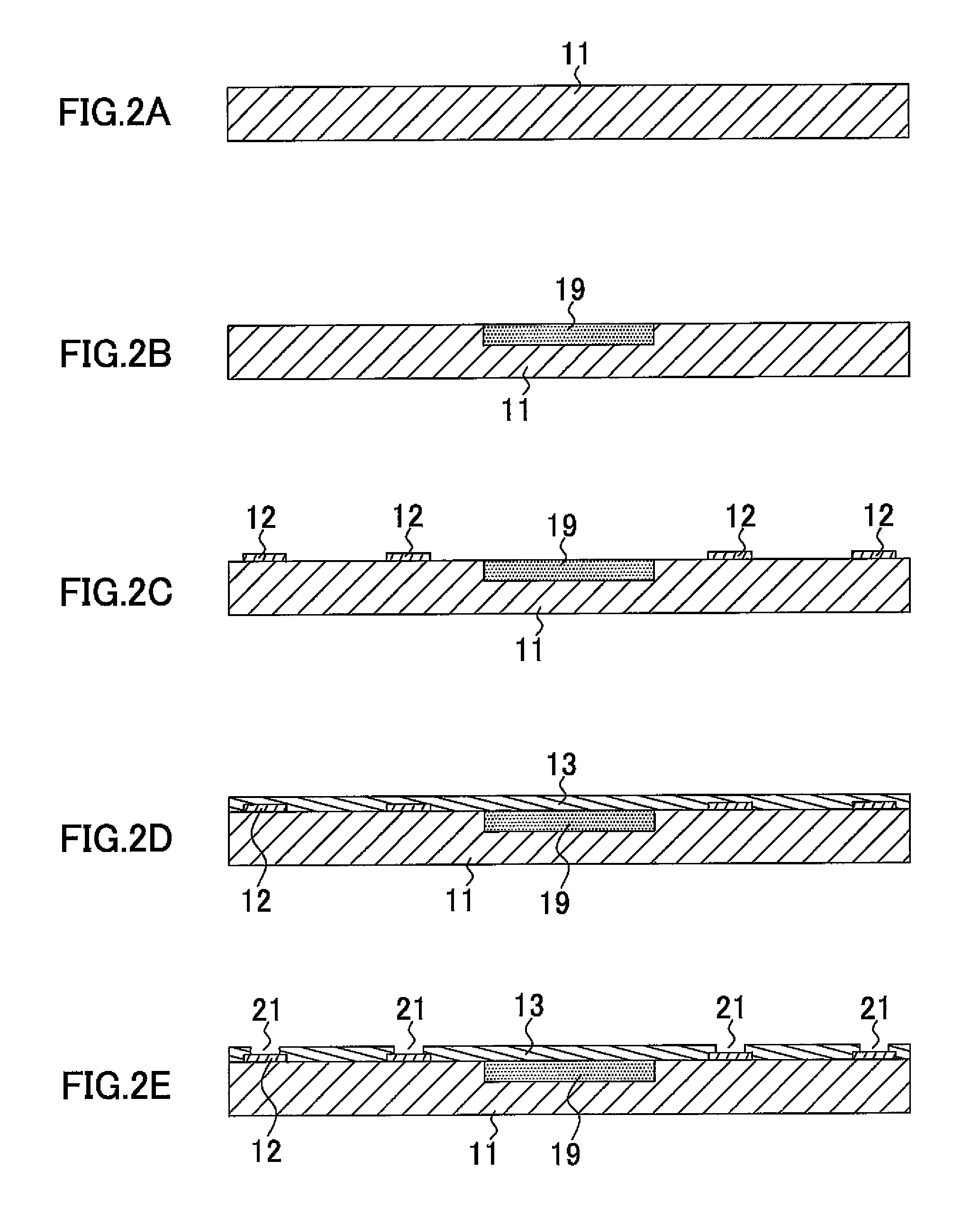
[0023]An embodiment of the present invention will be described in detail below with reference to the accompanying drawings.

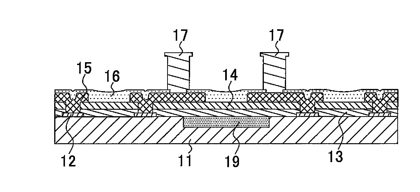
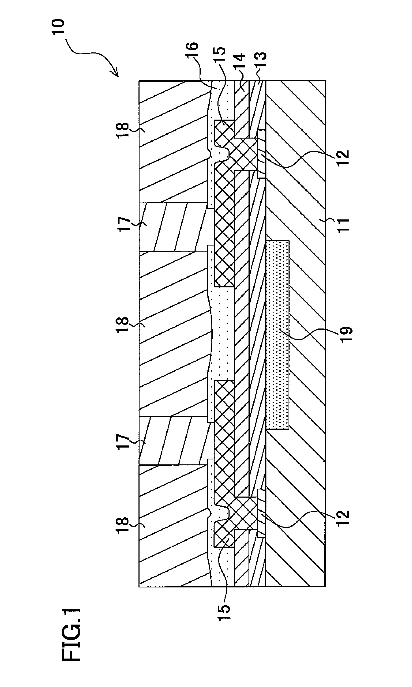
[0024]First, the structure of a semiconductor device formed by a semiconductor device manufacturing method that is an embodiment of the present invention will be described with reference to FIG. 1. FIG. 1 is a cross-sectional view of the semiconductor device formed by the semiconductor device manufacturing method that is the embodiment of the present invention.

[0025]As shown in FIG. 1, the semiconductor device 10 comprises a p-type silicon substrate 11 that is a semiconductor substrate, connection pads 12, an insulating film 13, a protective film 14, redistribution lines (also, referred to as sub-lines or sub-wirings) 15, a coating film 16, column-like external connection electrodes 17 (hereinafter, referred to as post bumps 17), and a sealing layer 18.

[0026]An integrated circuit portion 19 having lines or wirings in a desired shape is formed in the p-type silic...


PUM


Abstract

A method of manufacturing a semiconductor device, forms connection pads electrically connected to integrated circuit portion formed in a semiconductor substrate, lays an insulating film and a protective film one over another, forms sub-lines electrically connected to the connection pads on the protective film, forms a coating film covering the sub-lines and the protective film, sticks a dry film onto the coating film, forms external connection electrodes externally connectable and electrically connected to the sub-lines, and removes the dry film and forms a sealing layer covering the coating film and side surfaces of the external connection electrodes.

Description

BACKGROUND OF THE INVENTION[0001]1. Field of the Invention[0002]The present invention relates to a method of manufacturing semiconductor devices, and particularly to a manufacturing method of semiconductor devices called CSPs (Chip Size Packages).[0003]2. Description of the Related Art[0004]In these years, electronic devices such as mobile phones, mobile computers, personal digital assistants (PDAs), home video cameras, and digital cameras, and the peripheral components of the electronic devices are being dramatically reduced in size and weight. In association with this market trend, demands for reduction in size, thickness, and weight and high density mounting onto fine wiring boards of semiconductor chips to be used in electronic devices are increasing. In order to meet these demands, the development of semiconductor devices of package sizes the same as or slightly larger than the chip sizes, so-called CSPs (Chip Size Packages), is attracting attention.[0005]Other than being ultra...

Claims


Application Information

Patent Timeline
Patent Type & Authority Patents(United States)
IPC IPC(8): H01L21/44
CPCH01L23/3114H01L23/3192H01L24/03H01L24/05H01L2224/0401H01L2224/05599H01L2224/274H01L2924/01004H01L2924/01013H01L2924/01014H01L2924/01015H01L2924/01022H01L2924/01029H01L2924/01078H01L2924/014H01L2924/14H01L2924/01005H01L2924/01006H01L2924/01033H01L2924/00014
Inventor YOSHIDA, KATSUJI
Owner LAPIS SEMICON CO LTD
Learn More