
Doped ceramic powder for use in forming capacitor anodes

a technology of ceramic powder and capacitor, which is applied in the direction of capacitor electrolytes/absorbents, conductive materials, electrical apparatus, etc., can solve the problems of capacitor damage or destruction, formation of electrically conductive paths, and inability to meet the rated voltage of 16, 20 or 35 volts,

Inactive Publication Date: 2010-07-20
AVX CORP
View PDF102 Cites 12 Cited by
  • Summary
  • Abstract
  • Description
  • Claims
  • Application Information

AI Technical Summary

Benefits of technology

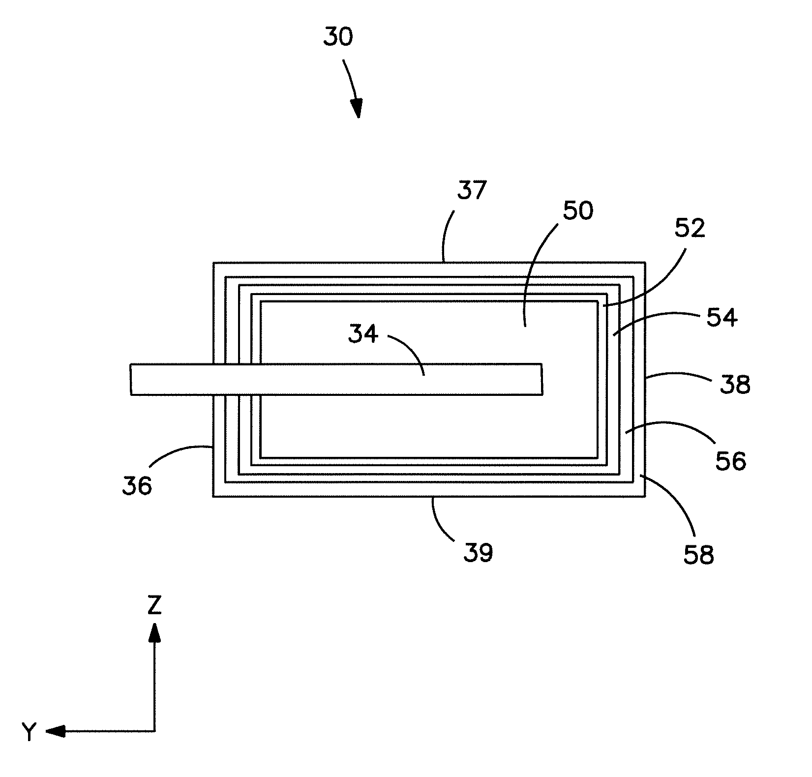
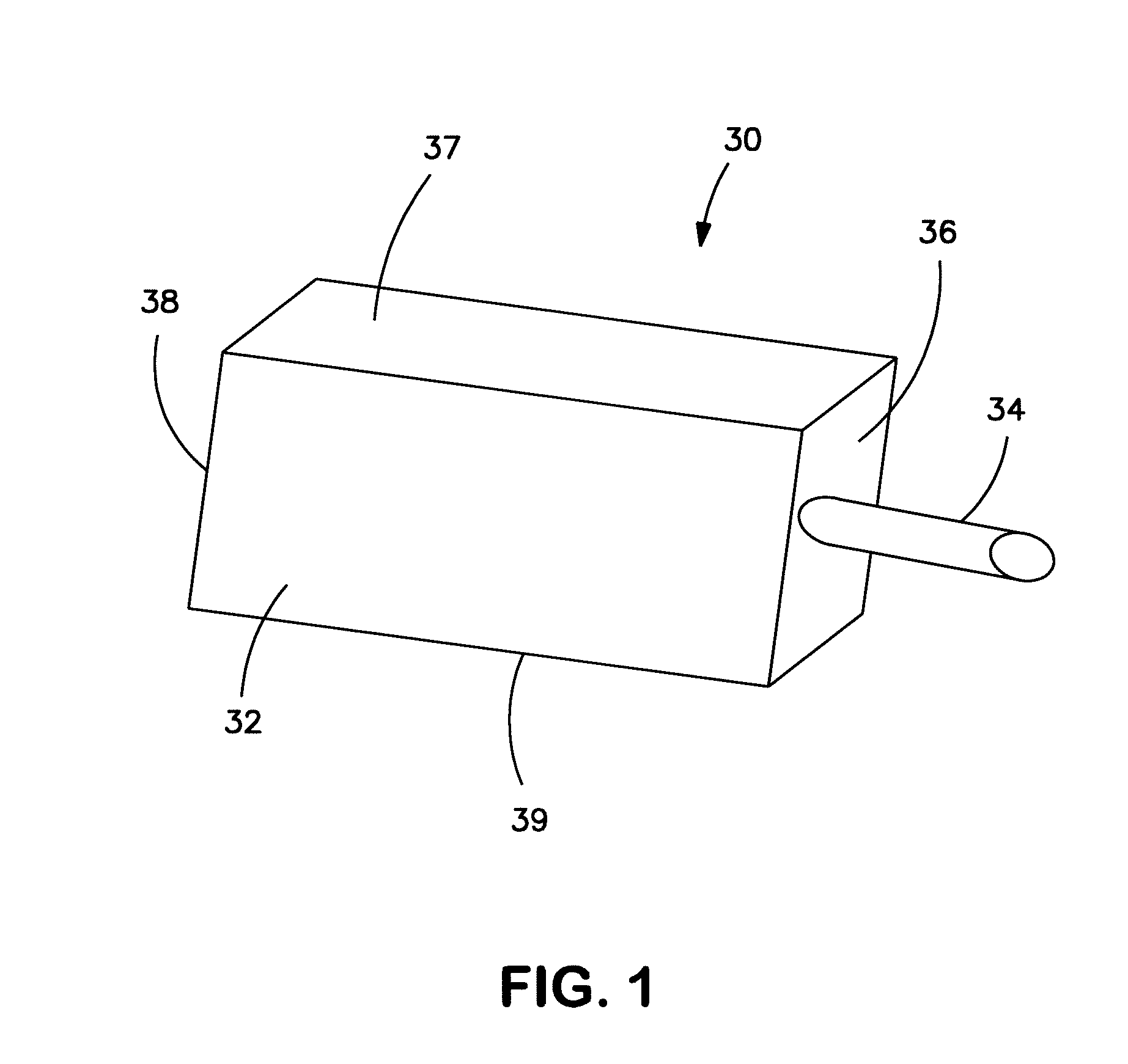
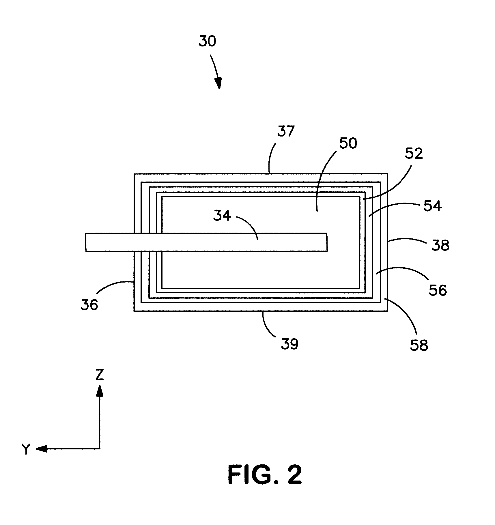
The present invention relates to an electrolytic capacitor with an anode body made from a powder containing electrically conductive ceramic particles and a non-metallic element. The non-metallic element has a ground state electron configuration with five valence electrons at an energy level of three or more. The capacitor also includes a dielectric layer and an electrolyte layer. The invention also provides a ceramic powder for use in the formation of capacitor anodes with a phosphorous content of about 200 parts per million or more. The method for forming a capacitor anode involves doping electrically conductive ceramic particles with a phosphorus dopant to form a powder with a phosphorous content of about 200 parts per million or more. The powder is compacted to form a pressed pellet and sintered. The technical effects of the invention include improved performance and reliability of the electrolytic capacitor.

Problems solved by technology

Despite the many benefits afforded by such ceramic-based (e.g., niobium oxide) capacitors, their use in high voltage applications (e.g., rated voltage of 16, 20 or 35 volts) has often been limited due to the relatively low breakdown strength of the dielectric.
Breakdown occurs quite abruptly (typically in nanoseconds), resulting in the formation of an electrically conductive path and a disruptive discharge through the material.
Capacitor damage or destruction can occur in such situations.
Unfortunately, it is believed that Schottky-type point defects are prevalent in the n-type semiconductor in which oxygen atoms leave their site in the lattice structure (thereby creating an oxygen vacancy) and move to the areas with lower concentration.
Those defects may form deep traps in the dielectric, which can store the electrical charge and serve as the source of charge carrier transport by Poole-Frenkel and tunneling mechanisms under the application of DC voltage.
The application of high voltage and temperature further accelerates the oxygen diffusion and increases the number of defects in dielectric.
This leads to leakage current instability at accelerated temperature and voltage load, which may limit the use of such capacitors at higher application voltages.

Method used


Image

  • Doped ceramic powder for use in forming capacitor anodes
  • Doped ceramic powder for use in forming capacitor anodes
  • Doped ceramic powder for use in forming capacitor anodes

Examples


example 1

[0041]NbO powder (HC Starck, 80,000 μF*V / g) was manually pre-mixed with niobium phosphide (325 mesh, Alfa Aesar) to obtain final phosphorous concentrations of 100, 200, 500, 1000 ppm. The resulting doped powder was homogenized in a Turbula® powder mixer. An aqueous solution was added to the dry powder that contained a polyethyloxazoline (“PX”) binder (2 wt. % PX based on the dry weight of the doped NbO powder). The binder solution and doped powder were manually mixed together. Thereafter, the powder was dried at 85° C. for 4 hours to evaporate the water. The powder was then embedded with a tantalum lead wire and pressed on a top / bottom press machine to a density of 3.4 g / cm3. The binder was then removed by placing the pellet into a nitrogen atmosphere at a temperature of 400° C. to 500° C. The pellet was then sintered at a temperature of 1520° C. for 10 minutes in an argon atmosphere.

[0042]To anodize the tantalum anode, it was dipped into a weak phosphoric acid / water solution having...

example 2

[0046]Capacitors were formed in the same manner as described in Example 1, except that the starting NbO(N) powder contained 3,000 parts per million of nitrogen. Once formed, various electrical parameters were measured and twenty-five (25) of the capacitors were subjected to life testing. The results are set forth below.

[0047]

PhosphorusNumber of DCLNitrogen contentcontentDCLrejects after life[ppm][ppm][μA]testing3,00000.10125 rej3,0001000.04525 rej3,0002000.12025 rej3,0005000.00125 rej3,0001,0000.05325 rej

[0048]Doping of NbO powder with phosphorus shows lower DCL results than in Example 1. It is expected that higher phosphorous concentrations would also lead to improved DCL stability.

example 3

[0049]Capacitors were formed in the same manner as described in Example 1, except that the starting NbO powder contained 5,000 parts per million of nitrogen. Once formed, various electrical parameters were measured and twenty-five (25) of the capacitors were subjected to life testing. The results are set forth below.

[0050]

PhosphorusNumber of DCLNitrogen contentcontentDCLrejects after life[ppm][ppm][μA]testing5,00000.10125 rej5,0001000.04525 rej5,0002000.12025 rej5,0005000.00125 rej5,0001,0000.05325 rej


PUM

PropertyMeasurementUnit
breakdown voltageaaaaaaaaaa
densityaaaaaaaaaa
densityaaaaaaaaaa

Abstract

An electrolytic capacitor that includes an anode body formed from a powder comprising electrically conductive ceramic particles and a non-metallic element in an amount of about 100 parts per million or more is provided in one embodiment of the invention. The non-metallic element has a ground state electron configuration that includes five valence electrons at an energy level of three or more. Examples of such elements include, for instance, phosphorous, arsenic, antimony, and so forth. The capacitor also comprises a dielectric layer overlying the anode body and an electrolyte layer overlying the dielectric layer.

Description

BACKGROUND OF THE INVENTION[0001]Electrolytic capacitors are often formed from valve action materials that are capable of being oxidized to form a dielectric layer. Typical valve action metals are niobium and tantalum. More recently, capacitors have been developed that employ an anode made from an electrically conductive oxide of niobium and a niobium pentoxide dielectric. Niobium oxide based capacitors have significant advantages over tantalum capacitors. For example, niobium oxide is more widely available and potentially less expensive to process than tantalum. Niobium oxide capacitors are also more stable against further oxidation and thus less prone to thermal runaway when over-voltaged (or otherwise over-loaded) than tantalum and niobium. Further, niobium oxide has several orders of magnitude higher minimum ignition energy compared to niobium and tantalum. Niobium oxide capacitors may also have a unique high resistance failure mechanism that limits the leakage current to a leve...

Claims


Application Information

Patent Timeline
Patent Type & Authority Patents(United States)
IPC IPC(8): H01G9/04H01G9/145
CPCC04B35/495H01G9/042H01G9/028C04B2235/42C04B2235/447C04B2235/608C04B2235/658C04B2235/6584C04B2235/727C22C1/05H01G9/0525H01G9/04
Inventor KARNIK, TOMAS
Owner AVX CORP
Learn More