Stacked film patterning method and gate electrode forming method

a gate electrode and film patterning technology, applied in the direction of basic electric elements, electrical equipment, semiconductor devices, etc., can solve the problems of affecting the uniformity of etching, and affecting the smooth etching progress, etc., to achieve high throughput, improve etching, and high anisotropy

Inactive Publication Date: 2010-05-25
NEC LCD TECH CORP
View PDF9 Cites 175 Cited by
  • Summary
  • Abstract
  • Description
  • Claims
  • Application Information

AI Technical Summary

Benefits of technology

[0024]In view of the above, it is a first object of the present invention to provide a stacked film patterning method and a gate electrode forming method which are capable of reliably removing residual substances remaining after etching of a metal film, improving etching uniformity of a silicon film, preventing the occurrence of an etching residue, and obtaining a TFT (Thin Film Transistor) having high reliability and excellent characteristics. It is a second object of the present invention to provide the stacked film patterning method and the gate electrode forming method which are capable of effectively removing residual substances remaining after etching of the metal film and of maintaining a high throughput. It is a third object of the present invention to provide the stacked film patterning method and the gate electrode forming method which are capable of preventing inconvenience of etching a region that needs to be left without being etched and accurately removing residual substances remaining after etching the metal film and of obtaining the TFT having high reliability and excellent characteristics.

Problems solved by technology

However, the method in which, after the wet-etching of the chromium film, the silicon film is dry etched has a problem; that is, an etching residue occurring after the wet-etching of the chromium film inhibits the dry-etching of the silicon film and, as a result, etching uniformity deteriorates and a residue of silicon occurs.
However, in a state in which the residues of metal chromium and / or the residual substances 110 being chromium silicide are left on the micro-crystal silicon film 106, these substances act as a mask which impairs the progress of smooth etching.
However, the conventional technologies have problems.
A first problem to be solved is that, in the above conventional technology, residual substances remaining after etching a metal film cannot be removed satisfactorily and, as a result, etching uniformity of a silicon film deteriorates and residues of etching occur.
That is, since a vapor pressure of an oxide of metal or silicon is low, the removal of residual substances by etching using only plasma of oxygen is impossible.
Moreover, by the repetition of both the oxygen plasma processing and subsequent silicon film etching processes, oxygen and an residual amount of gas used for etching the silicon film are mixed and, as a result, though the effect of removing residual substances appears, the residual amount of the gas used for etching the silicon film, decreases during the evacuation and oxygen plasma processing to be carried out before subsequent processing on a substrate starts and the capability of removing the residual substances becomes unstable and the effect of removing residual substances decreases with passage of processing time.
Also, when the technology disclosed in the above Japanese Patent Application Laid-open No. 2001-274411 is applied to the formation of a gate electrode of a top-gate type polycrystalline TFT, the residual substances cannot be fully removed in patterning of a stacked film made up of a metal film formed on a polycrystalline silicon film or micro-crystal silicon film having a crystalline property being higher than that of amorphous silicon.
Additionally, in a region in which the polycrystalline silicon film serving as the active layer exists with the gate insulating film being interposed between the micro-crystal silicon film and the polycrystalline silicon film under the gate electrode of the top-gate polycrystalline TFT, concave and / or convex portions occurring on the surface of the silicon film of the gate electrode are big in size and complicated in shape.
If residual substances increase, even by the etching process using plasma of a mixed gas including CHF3 gas and oxygen gas, it is impossible to fully remove residual substances.
A second problem to be solved is that the above conventional technology causes a decrease in throughput.
Hei 06-283547, successive processes of the wet-etching process using the solution including hydrofluoric acid and the subsequent process of etching the silicon film are impossible, which causes a decrease in throughput.
Moreover, a third problem to be solved is that, in the conventional technology, etching of a region that should be left without being etched or a similar unexpected matter occurs; that is, by the conventional technology, exact removal of residual substances is impossible.
Hei 06-283547, when the wet-etching process is performed using the solution including hydrofluoric acid, if the solution being highly capable of removing residual substances of metal and / or metal silicide is used, a phenomenon of side-etching of a metal film occurs during the process, which also makes it impossible to maintain a desired pattern shape of the metal film.
Since anisotropy is very strong in the sputter-etching, in a place where steps exist, removal of residual substances existing on a side of the step portion is difficult.

Method used


Image

  • Stacked film patterning method and gate electrode forming method
  • Stacked film patterning method and gate electrode forming method
  • Stacked film patterning method and gate electrode forming method

Examples


first embodiment

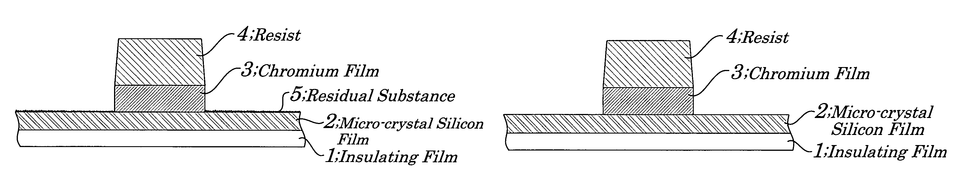
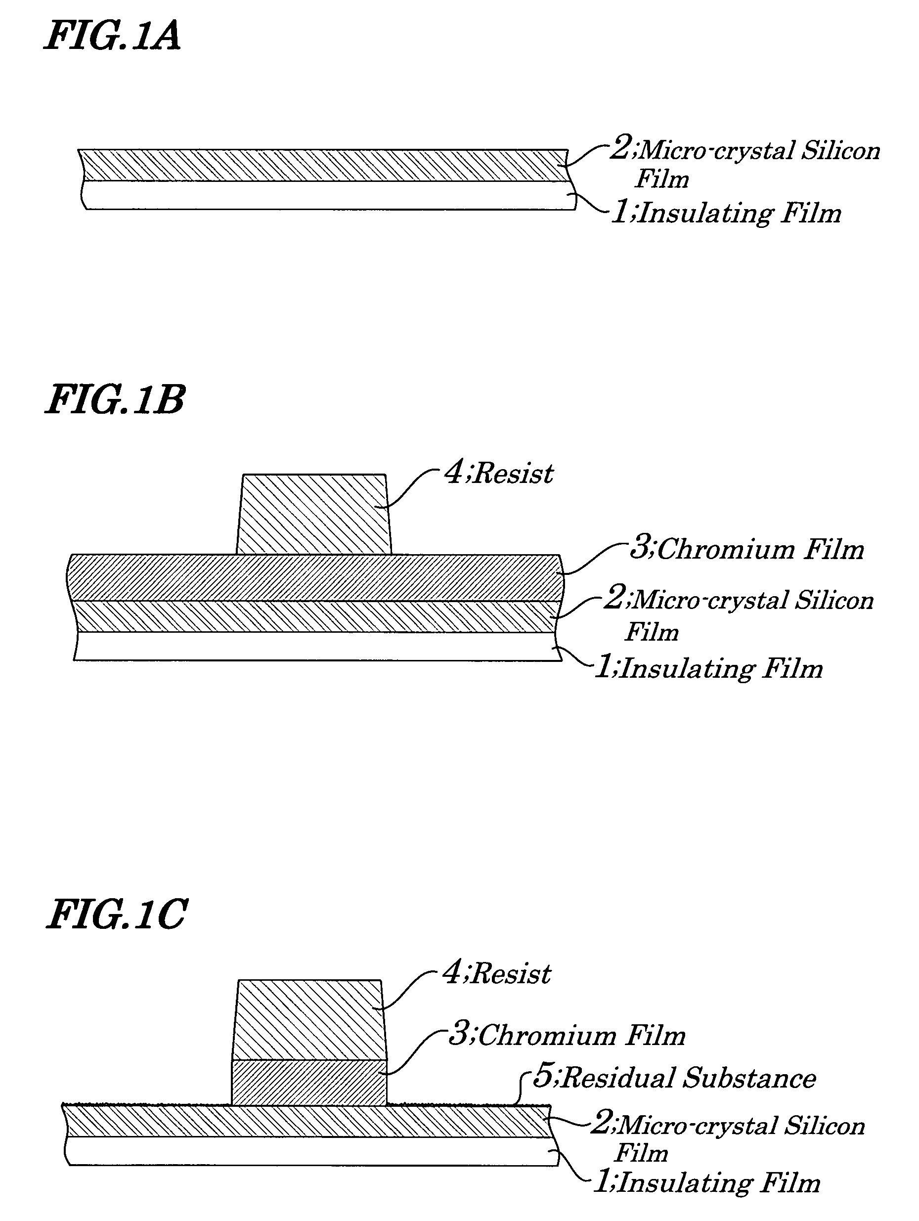
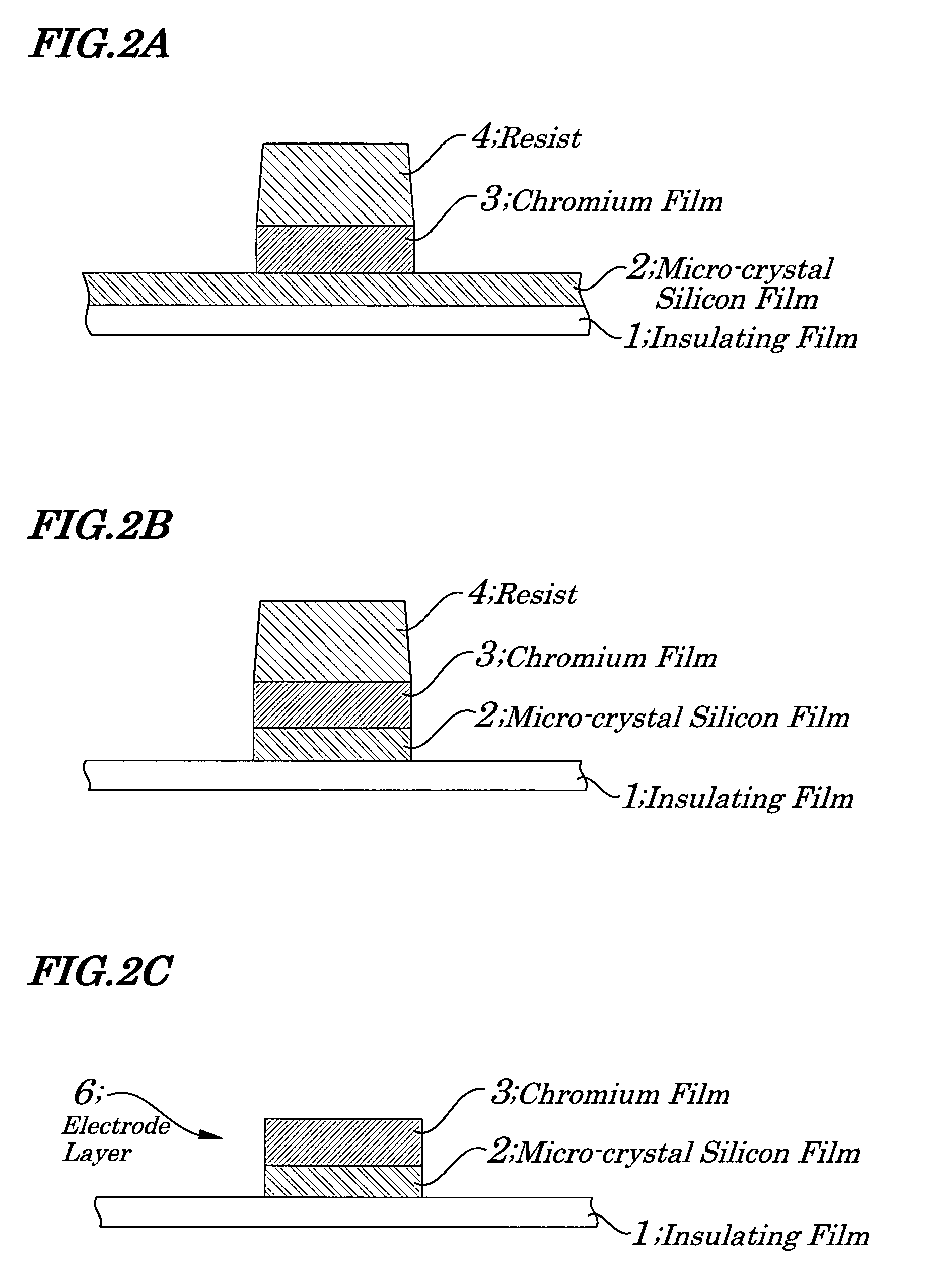
[0066]FIGS. 1A to 1C are process diagrams explaining a stacked film patterning method of the first embodiment of the present invention. FIGS. 2A to 2C are also process diagrams explaining the stacked film patterning method of the first embodiment. FIG. 3 is a diagram schematically showing configurations of a dry-etching apparatus to be used to perform the stacked film patterning method of the first embodiment. The stacked film patterning method of the first embodiment is used to form an electrode layer 6 which is a stacked film having a two-layer structure in which a metal film is stacked on a silicon film deposited on an insulating film 1 formed on a substrate (see FIG. 2C).

[0067]First, as shown in FIG. 1A, an n-type micro-crystal silicon film 2 including phosphorus as an impurity is deposited as a silicon film so as to have a film thickness of about 100 nm by a PECVD (Plasma Enhanced Chemical Vapor Deposition) method on the insulating film 1 made of silicon dioxide formed on a sub...

second embodiment

[0080]FIGS. 4A to 4C are diagrams explaining a stacked film patterning method according to the second embodiment of the present invention. The method of the second embodiment differs greatly from that of the first embodiment in that wet etching is performed to a mid point of a thickness of a chromium film (so as to reach a specified depth of the film). Configurations other than above are the same in the first embodiment and same reference numbers are assigned to components having the same function as in the first embodiment and their descriptions are simply made in FIGS. 4A to 4C accordingly.

[0081]First, as shown in FIG. 4A, a micro-crystal silicon film 2 as a silicon film is formed so as to have its film thickness of about 100 nm on an insulating film 1 made of silicon dioxide or a like. Next, a chromium film 3 as a metal film is deposited so as to have its film thickness of about 200 nm.

[0082]Then, the chromium film 3 is wet etched using a resist as a mask and using an ammonium ce...

third embodiment

[0088]FIGS. 5A, 5B, and 5C and FIGS. 6A, 6B, and 6C are process diagrams explaining a method of manufacturing polycrystalline TFTs according to the third embodiment of the present invention. The method of the third embodiment is a method for manufacturing a gate electrode making up a polycrystalline silicon TFT in which the stacked film patterning method provided in the first and second embodiments is used. As a gate electrode layer, two-layer stacked film made up of a metal film deposited on a silicon film is formed on a gate insulating film by patterning and, as a semiconductor layer, polycrystalline silicon (p-Si) is used.

[0089]First, as shown in FIG. 5A, in order to prevent contamination caused by metal or a like on a glass substrate 21, a front-end insulating film 22 made of silicon dioxide or silicon nitride with its film thickness of about 300 nm is deposited on the glass substrate 21 by a plasma CVD or reduced pressure CVD. Next, an amorphous silicon (a-Si) film 23 is deposi...


PUM


Abstract

A stacked film patterning method is provided which is capable of reliably removing residual substances remaining after etching of a metal film, improving etching uniformity of a silicon film, and preventing an occurrence of etching residues. A micro-crystal film and a chromium film are sequentially formed on an insulating film serving as a front-end film and the chromium film is etched to be patterned by using a resist as a mask. Next, a micro-crystal silicon film on which the residual substances exist is exposed to plasma of a mixed gas including chlorine gas and oxygen gas to selectively etch the residual substances on a surface of the micro-crystal silicon film. After that, the micro-crystal silicon film is dry etched.

Description

INCORPORATION BY REFERENCE[0001]This application is based upon and claims the benefit of priority from Japanese Patent Application No. 2006-137112, filed on May 16, 2006, the disclosure of which is incorporated herein in its entirely by reference.BACKGROUND OF THE INVENTION[0002]1. Field of the Invention[0003]The present invention relates to a stacked film patterning method and a gate electrode forming method and more particularly to the stacked film patterning method to be used in manufacturing of, for example, a TFT (Thin Film Transistor) substrate making up a liquid crystal display device and to be used when a stacked film with a two-layer structure configured by stacking a metal film on a silicon film is formed as, for example, an electrode layer and to the method of forming the gate electrode of, for example, the TFT.[0004]2. Description of the Related Art[0005]Conventionally, a structure of a TFT is classified into two types, one being of a bottom-gate type to be used mainly i...

Claims


Application Information

Patent Timeline
IPC IPC(8): H01L21/3205
CPCH01L29/66757H01L29/4908
Inventor HAYASHI, KENICHI
Owner NEC LCD TECH CORP
Why Eureka
Try Eureka