
Method for forming image through reaction development

a technology of reaction development and photoresist, which is applied in the field of photoresist technology, can solve the problems of low molecular weight polymers and dissolution, and achieve the effect of low environmental load

Inactive Publication Date: 2009-12-29
YOKOHAMA TLO
View PDF10 Cites 0 Cited by
  • Summary
  • Abstract
  • Description
  • Claims
  • Application Information

AI Technical Summary

Benefits of technology

"The present invention is a new method for developing a pattern on a photo resist layer using a special type of polymer and a photo acid generating agent. This method allows for the use of polymers containing carbonyl groups without needing to have special functional groups that can react with a base or an acid. The method uses a mixture of an amine and at least one of water and organic solvents as the solvent solution. The polymer can contain carbonyl groups in the main chain, which are then broken when exposed to ultraviolet light. This process results in low molecular weight polymers that dissolve in the development solution. The invention also includes a formed material (photo resist molded material) formed using this method and semiconductor integrated circuits, printed wire substrates, liquid crystal panels, and photo wave guide path devices containing this formed material. The method is characterized by its ability to destroy bonds with low reactivity toward nucleophilic reagents and its ability to use polymers containing carbonyl groups with low reactivity toward nucleophilic reagents."

Problems solved by technology

The breakage in the main chain results in low molecular weight polymers, which dissolve in the development solution.

Method used


Image

  • Method for forming image through reaction development
  • Method for forming image through reaction development
  • Method for forming image through reaction development

Examples


example 1

[0054]Twenty grams of bisphenol A type polycarbonate (henceforth referred to as PC) in the form of pellets was added to a 200 ml pear-shaped flask with 60 g of NMP. The contents were mechanically agitated at 180° C. to heat and dissolve the solids to obtain an NMP varnish of PC (the solids content: 25% by weight). Next, 20 g of the varnish was added to a solution obtained by dissolving 1.5 g of diazonaphthoquinone type photo sensitizer PC-5 (Toyo Gosei, 1,2-naphthoquinone-2-diazide-5-sulfonic acid p-cresol ester) in 5 g of NMP, and a photo resist formulation (a light sensitive PC composition) was prepared by agitating the mixture with a stirrer for about an hour at room temperature. This solution was spin coated (600 rpm / 10 seconds+1,000 rpm / 30 seconds) on a 35 μm electrolytic copper foil (on shiny or matte surface). The coating was pre-baked (90° C. / 10 minutes) using a far infrared hot air circulating type dryer to obtain a photosensitive PC coating film 15 μm thick. An ultraviolet...

example 2

[0055]Polyarylate (Unitika, U polymer, henceforth referred to as PAr) was used in place of PC, but the same operations described in Example 1 were used to prepare a photo resist formulation.

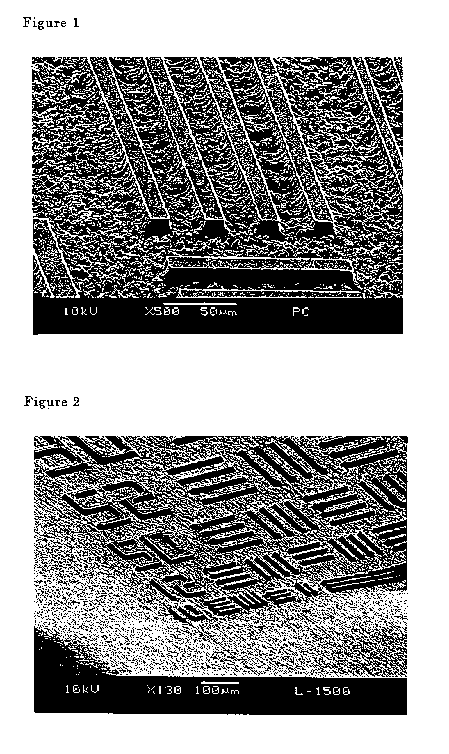
[0056]This photo resist formulation was used to execute the same operations described in Example 1 to obtain a photosensitive coating film, 15 μm thick. Next, a developing solution comprising 400 g of ethanolamine, 100 g of NMP and 100 g of ion exchanged water was used, and the image was developed for twelve minutes at 45° C. The same operations described in Example 1 were conducted to obtain a positive image. The degree of resolution was 10 μm in terms of a line-and-space pattern. The SEM photograph of this photo resist is shown in FIG. 2.

example 3

[0057]The same operations described in Example 1 were used to prepare a photo resist formulation (PC).

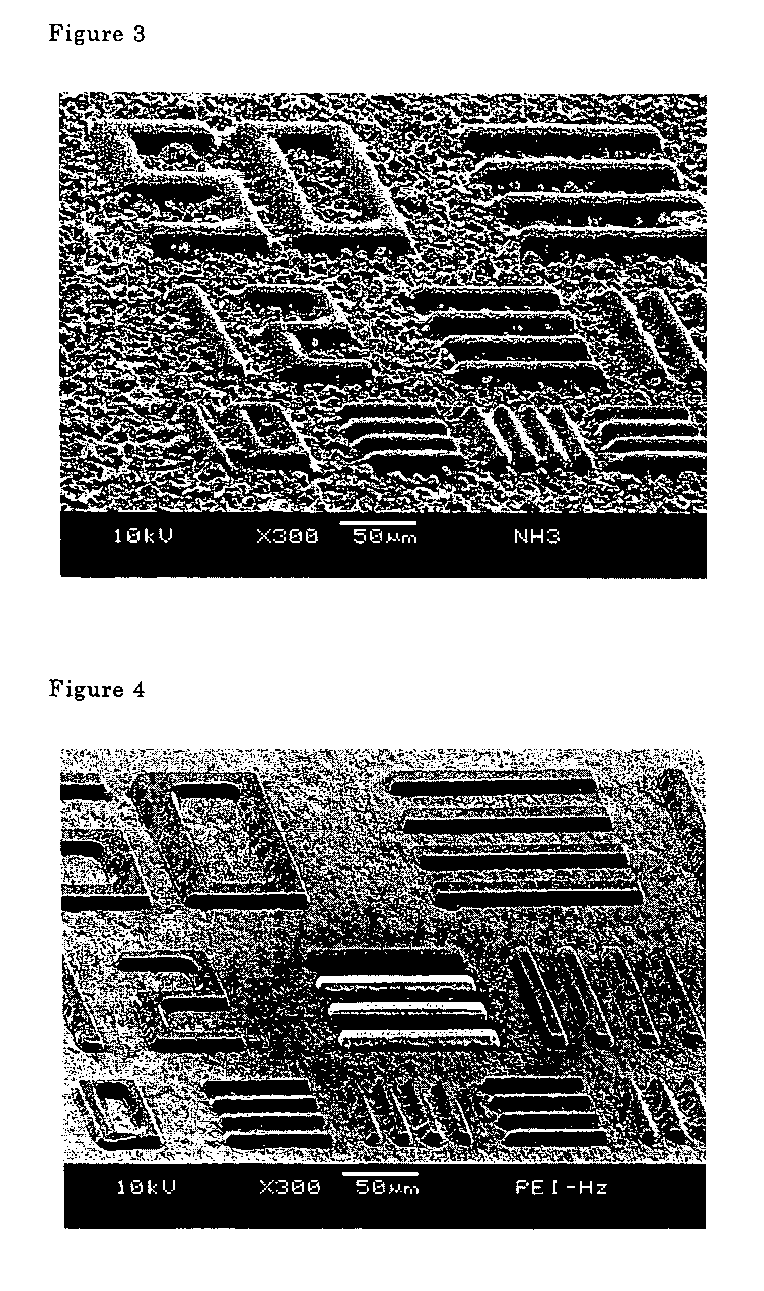
[0058]This photo resist formulation was used to execute the same operations described in Example 1 to obtain a photosensitive coating film 14 μm thick. An exposure rate of 2,000 mJ / cm2 was used, and a developing solution comprising 100 g hydroxylamine, 100 g of NMP and 100 g of ion exchanged water was used to develop an image for seven minutes at 41° C. The same operations described in Example 1 were conducted to obtain a positive image. The degree of resolution was 20 μm in terms of a line-and-space pattern.


PUM

PropertyMeasurementUnit
thicknessaaaaaaaaaa
thicknessaaaaaaaaaa
temperatureaaaaaaaaaa

Abstract

The invention relates to a reaction development patterning process wherein a photo resist layer masked by a desired pattern is irradiated using ultraviolet light and this layer is subsequently washed using a solvent solution containing alkali characterized by said photo resist layer comprising a condensation type polymer containing in the main chain carbonyl groups (C═O) bonded to hetero atoms and a photo acid generating agent and said alkali being an amine. This reaction development patterning process is characterized by being able to use as a photo resist target resins containing bonds having low reactivity toward nucleophilic reagents, for example, condensation type polymers containing any one of bonds such as carbonate, ester, urethane and amide.

Description

TECHNICAL FIELD OF THE INVENTION[0001]This invention relates to a photo resist technology that can be used to manufacture semiconductor integrated circuits, printed wire substrates and liquid crystal panels, more specifically, to a photo resist technology to form a positive image with a reactive alkali development solution by making a film with a condensation type polymer and a photo acid generating agent and irradiating ultraviolet light.PRIOR ART[0002]Photo resist technology is usually, in a technology field related to photographic plate processing, applied to organic polymers capable of photo molding that are used to manufacture printed electronic circuits and printed circuit substrates or to manufacture semiconductor laminates with microelectronic engineering.[0003]In order to create a circuit structure when manufacturing semiconductor integrated parts using microelectronic engineering, a semiconductor substrate generates a photo resist relief structure, by exposing a photo resi...

Claims


Application Information

Patent Timeline
Patent Type & Authority Patents(United States)
IPC IPC(8): G03F7/00G03F7/004G03F7/023G03F7/039G03F7/32
CPCG03F7/0233G03F7/039G03F7/322G03F7/0392Y10S430/114
Inventor TOMOI, MASAOFUKUSHIMA, TAKAFUMIITATANI, HIROSHI
Owner YOKOHAMA TLO
Learn More