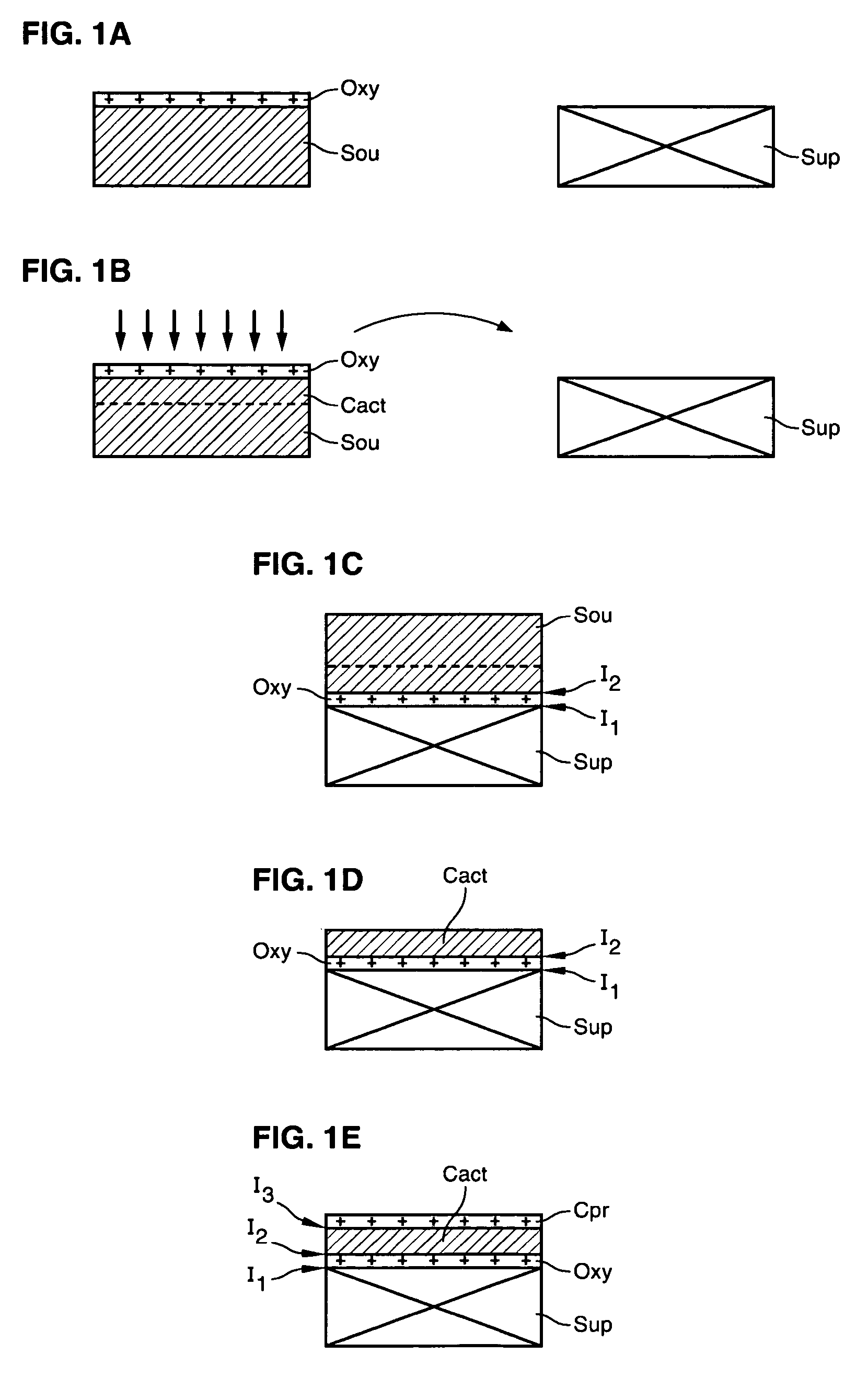
Method of fabricating a composite substrate with improved electrical properties
a technology of composite substrates and electrical properties, applied in the direction of sustainable manufacturing/processing, climate sustainability, final product manufacturing, etc., can solve the problems of fga treatment methods losing effectiveness at each encountered interface, trapping can have an extremely deleterious impact on the electrical properties of any future electronic components, etc., and achieve good electrical properties
- Summary
- Abstract
- Description
- Claims
- Application Information
AI Technical Summary
Benefits of technology
Problems solved by technology
Method used
Image
Examples
example 1
Preparation of a Substrate Including an Active Layer that Comprises a Ground Plane (Known by the Acronym “GP-SOI”, or “Ground Plane Silicon on Insulator”)
[0094]This example will be described with reference to FIGS. 3A to 3G. A silicon support substrate 1 was covered with a deposit of a thin layer 60 about 1 micrometer (μm) thick and highly doped with boron (see FIGS. 3A and 3B), to define a ground plane therein.
[0095]This highly doped layer had a front face 600 that was used for bonding (see FIG. 3C). Front face 600 was polished or smoothed to reduce its roughness and render front face 600 to render front face 600 compatible with bonding.
[0096]As shown in FIG. 3D, support substrate 1 was covered with a doped layer 60 and then underwent a high temperature thermal annealing treatment or RTA, typically at 1050° C. for about 10 seconds. Further, a silicon source substrate 2 was used, oxidized by dry oxidation.
[0097]Silicon source substrate 2 was covered with a layer 32 of SiO2 about 50 ...
example 2
Preparation of a Composite Substrate Comprising an Active Layer of Silicon on a Stack of Oxide and Quartz
[0102]The same type of source substrate 2 used in Example 1 was employed in Example 2. It underwent the same treatments, with the exception of the recovery treatment that was carried out by a high temperature anneal at 1100° C., and the formation of the zone of weakness was carried out by co-implantation of helium using a dose of 1.5×10¹⁶He+ / cm2 and hydrogen using a dose of 1×10¹⁶H+ / cm2.
[0103]Further, a quartz support substrate 1 comprising a front face 10 that underwent plasma activation using the parameters used in Example 1 for substrate 2 was used.
[0104]The composite substrate thus obtained had DIT values at the interface between the oxide and the silicon of the order of several 1010·eV−1·cm−2.
[0105]In accordance with the invention, the fact that the recovery treatment was carried out systematically prior to plasma activation meant that the bonding energy was not reduced but ...
PUM
| Property | Measurement | Unit |
|---|---|---|
| temperature | aaaaa | aaaaa |
| temperature | aaaaa | aaaaa |
| pressure | aaaaa | aaaaa |
Abstract
Description
Claims
Application Information
 - R&D
- Intellectual Property
- Life Sciences
- Materials
- Tech Scout
- Unparalleled Data Quality
- Higher Quality Content
- 60% Fewer Hallucinations
Browse by: Latest US Patents, China's latest patents, Technical Efficacy Thesaurus, Application Domain, Technology Topic, Popular Technical Reports.
© 2025 PatSnap. All rights reserved.Legal|Privacy policy|Modern Slavery Act Transparency Statement|Sitemap|About US| Contact US: help@patsnap.com


