
Plasma processing apparatus, semiconductor manufacturing apparatus and electrostatic chucking unit used thereof

a technology of electrostatic chucking and processing apparatus, which is applied in the direction of chucks, mechanical apparatus, manufacturing tools, etc., can solve the problems of plasma damage, plasma damage produced in a wafer due to strains in the electric field at the beginning of bias rf application, and product yield remarkably lowered, so as to improve device yield, reduce electric field in vacuum chamber, and reduce the effect of electric field strain

Inactive Publication Date: 2008-07-01
RENESAS ELECTRONICS CORP
View PDF9 Cites 5 Cited by
  • Summary
  • Abstract
  • Description
  • Claims
  • Application Information

AI Technical Summary

Benefits of technology

The present invention provides a plasma processing apparatus with an electrostatic chuck unit for supporting and processing an object using RF bias. The apparatus includes a bias introducing rod and a wiring member that is electrically connected to the rod and taken out with spacing from the chuck unit. The wiring member is symmetrically arranged on the chuck unit to ensure uniform electric field distribution and reduce plasma damage to the object being processed. The technical effect of the invention is to improve the yield of devices and reduce plasma damage during processing.

Problems solved by technology

In addition, where plasma processing is carried out by generating high-power and high-density plasma using the electrostatic chuck of the second prior art, it has been pointed out that unfavorable damage occurs in a substrate to be plasma-treated, for example, a semiconductor wafer, and as a result, product yield is remarkably lowered.
On the other hand, it has been pointed out, in the second prior art, that the electric field in the vacuum chamber is locally increased due to overlapping of the electric field based on the source RF output portion and the electric field generated in the application position of the bias RF in the ESC stage, whereby plasma is biased, and plasma damage is produced at a partial area of silicon wafer.
However, the second prior art only points out alternation of the positions of the source RF output portion and the bias RF application point.
The second prior art does not disclose any means for making uniform the electric field inside the ESC stage.
Further, according to experiments made by the present inventor, as in the second prior art, it is made clear that only alteration of the connection position of the bias RF wiring connected to the RF introduction rod is insufficient to make distribution of the electric field in the vacuum chamber uniform.
Since the larger the antenna ratio becomes, the wider the area exposed to plasma becomes, deterioration of the gate breakdown voltage becomes remarkable.
In addition, in a case of a device having a fixed antenna ratio, the higher the intensity of plasma is, the greater the deterioration of the gate breakdown voltage of the device becomes.

Method used


Image

  • Plasma processing apparatus, semiconductor manufacturing apparatus and electrostatic chucking unit used thereof
  • Plasma processing apparatus, semiconductor manufacturing apparatus and electrostatic chucking unit used thereof
  • Plasma processing apparatus, semiconductor manufacturing apparatus and electrostatic chucking unit used thereof

Examples


Embodiment Construction

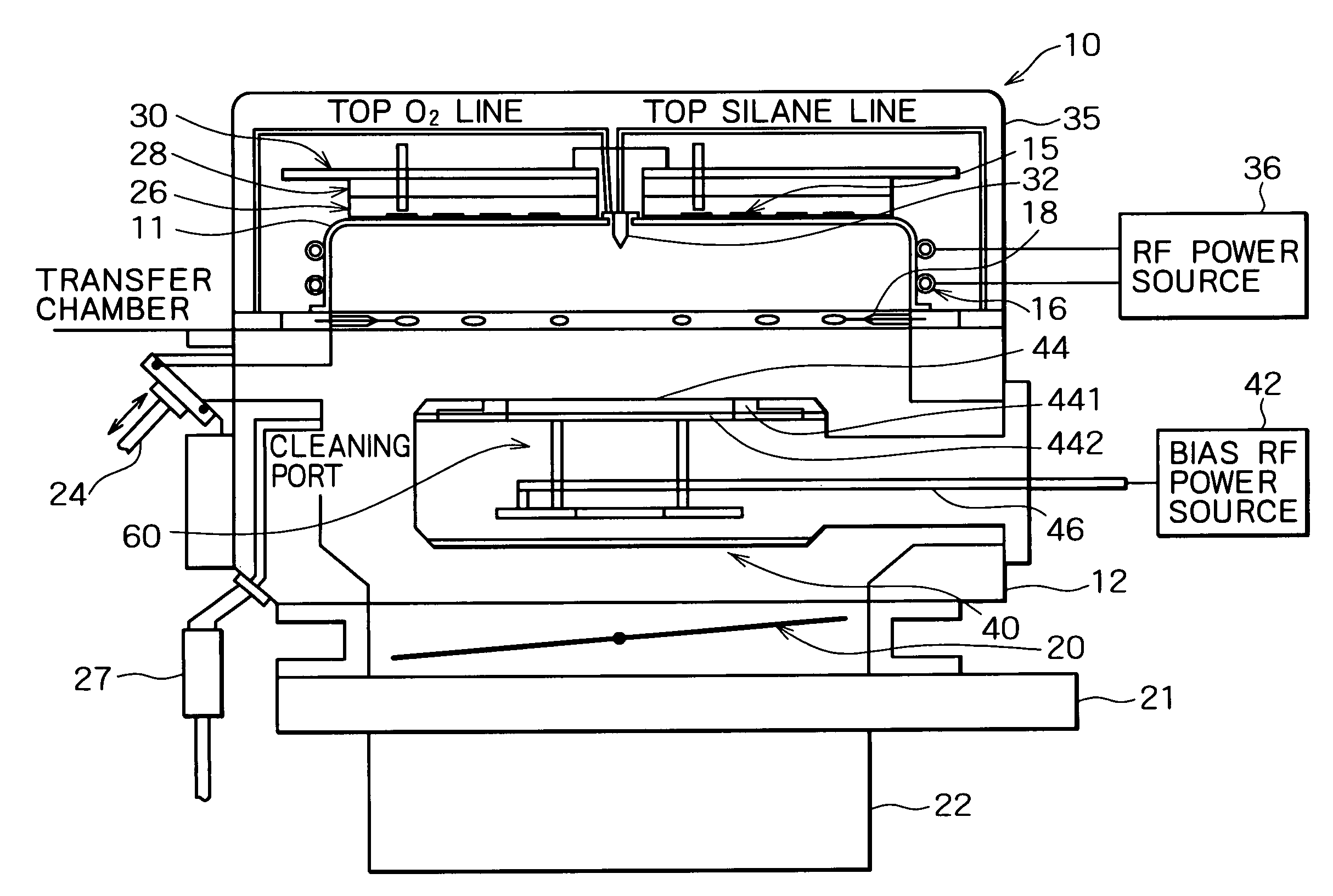
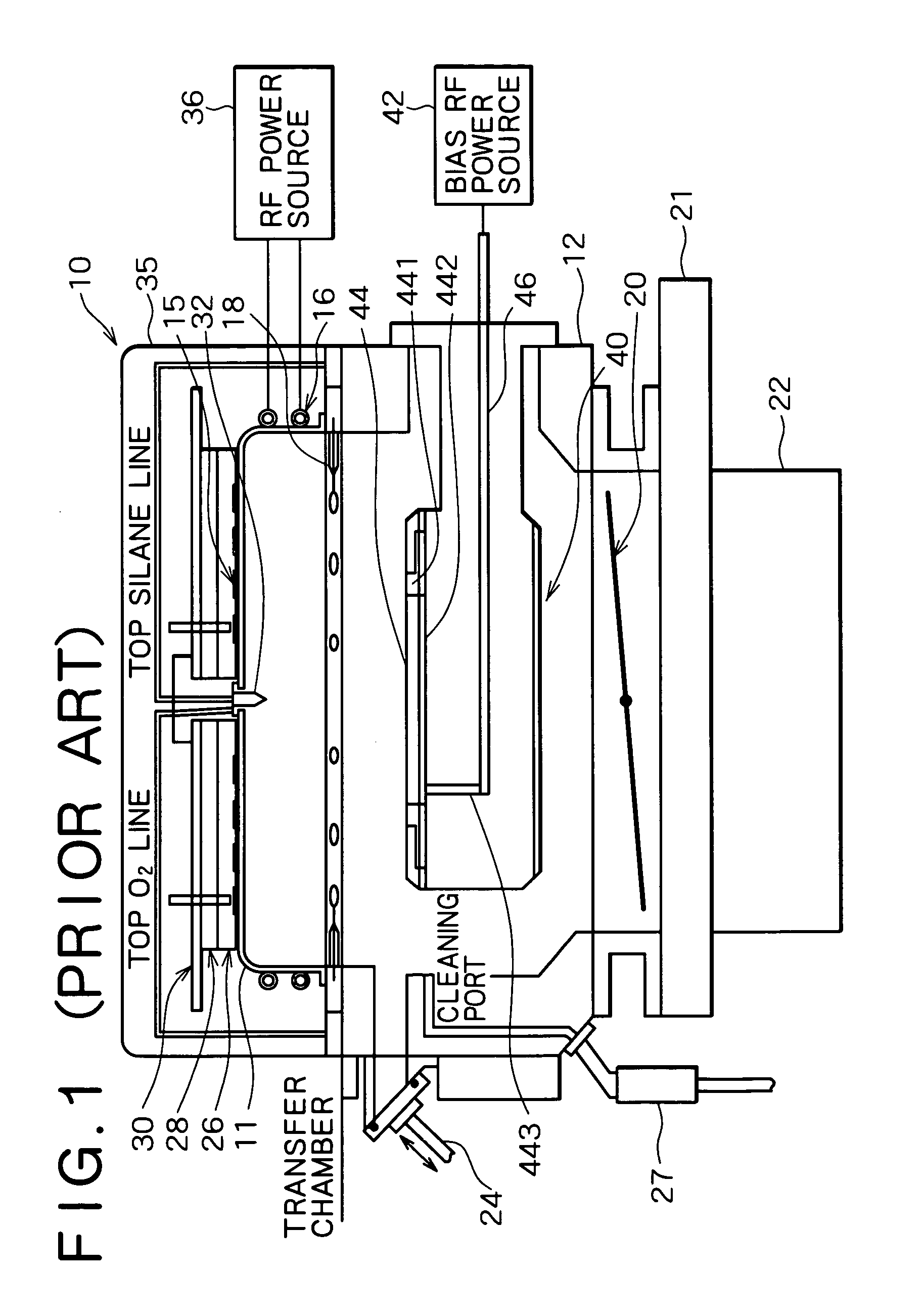
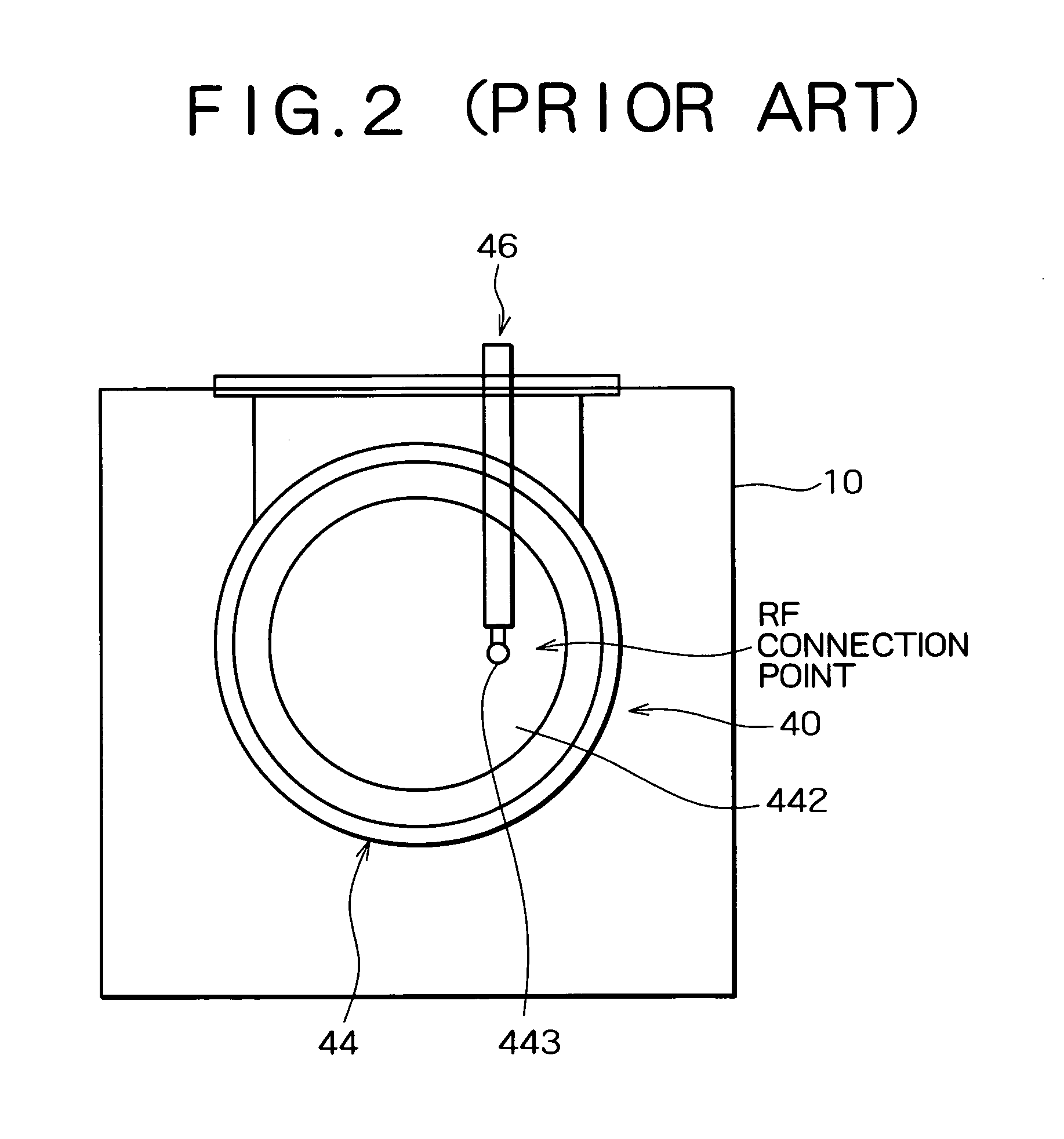
[0043]In the HDP-CVD apparatus shown in FIG. 1 and FIG. 2, the present inventors carried out experiments in which an electrostatic chuck unit 44 and a wiring member 443 are connected to each other in a plurality of positions and conducted an evaluation using antenna ratios. At this time, experiments and evaluation using the antenna ratio, which are similar to the above, were carried out while varying the shape of the wiring member 443 and simultaneously changing the number of connection positions between the electrostatic chuck unit 44 and the wiring member 443. As a result, it was found that the shape of the wiring member influences generation of plasma damage on a semiconductor wafer. In other words, it is found that, by shaping the wiring member so as to become substantially symmetrical to the RF introduction rod, asymmetry of the electric field by the bias RF can be improved, and influences due to plasma damage can be reduced. Further, such a finding could be obtained, that gene...


PUM

PropertyMeasurementUnit
breakdown voltageaaaaaaaaaa
conductiveaaaaaaaaaa

Abstract

A wiring member which becomes substantially symmetrical on the plane of an electrostatic chuck unit is connected to the tip end of an RF introduction rod between the RF introduction rod and the electrostatic chuck unit in order to make uniform generation of an electric field due to bias RF which becomes a cause of plasma damage. The connection point between the electrostatic chuck unit and the wiring member may be single or plural.

Description

BACKGROUND ART OF THE INVENTION[0001]1. Technical Field[0002]The present invention relates to a plasma processing apparatus for processing an object to be treated, in particular a semiconductor wafer or a substrate for liquid crystal, a semiconductor manufacturing apparatus such as a high-density plasma (HDP) CVD apparatus, and an electrostatic chucking unit used for the corresponding semiconductor manufacturing apparatus.[0003]2. Related Arts[0004]Generally, a plasma etching apparatus, plasma CVD apparatus, ion implantation apparatus, sputtering apparatus, etc., are available as a plasma processing apparatus used for manufacturing semiconductor devices, liquid crystal display devices, etc. A high-density plasma (HDP)-CVD apparatus, which carries out CVD (chemical vapor deposition) by generating high-concentration plasma, of these plasma processing apparatuses is used for forming an interlayer insulation film, trench embedding film, or passivation film in a semiconductor apparatus.[...

Claims


Application Information

Patent Timeline
Patent Type & Authority Patents(United States)
IPC IPC(8): C23C16/00B23B5/22B25G3/22C23F1/00H01L21/306H01L21/683H01T23/00C23C16/458C23C16/507C23C16/513H01L21/00H01L21/31
CPCC23C16/4586C23C16/507H01J37/32577H01L21/67069H01L21/6831H01J37/32706Y10T279/23
Inventor TANIKUNI, TAKAMASADEN, YASUHIDE
Owner RENESAS ELECTRONICS CORP
Learn More