
Ultra-wideband receiver and transmitter

Inactive Publication Date: 2007-04-24
ZEBRA TECH CORP
View PDF13 Cites 75 Cited by
  • Summary
  • Abstract
  • Description
  • Claims
  • Application Information

AI Technical Summary

Benefits of technology

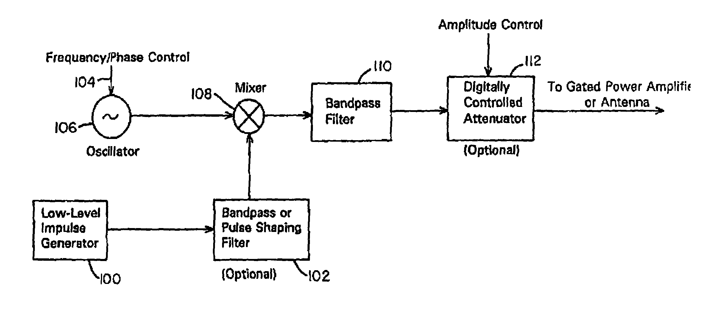
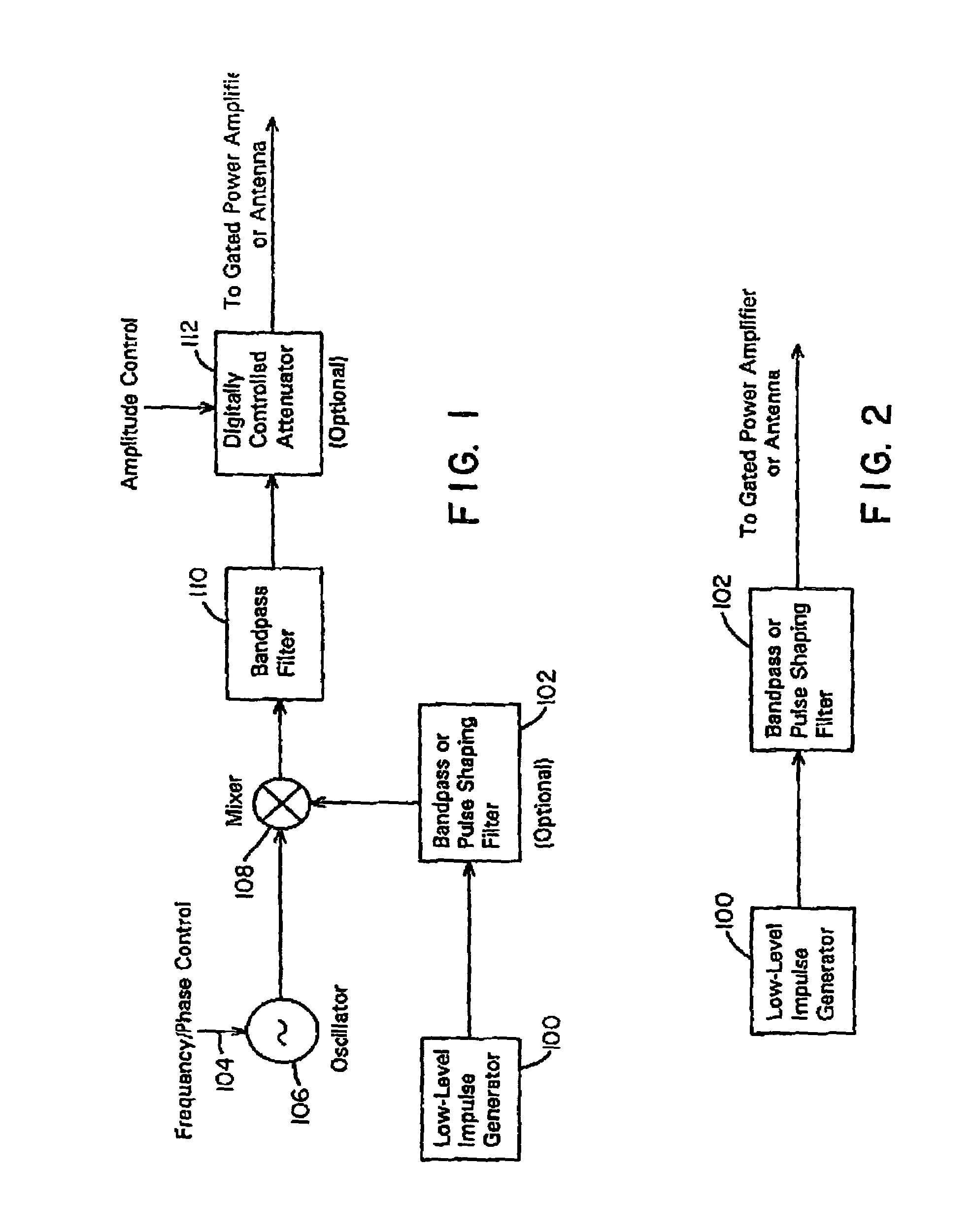
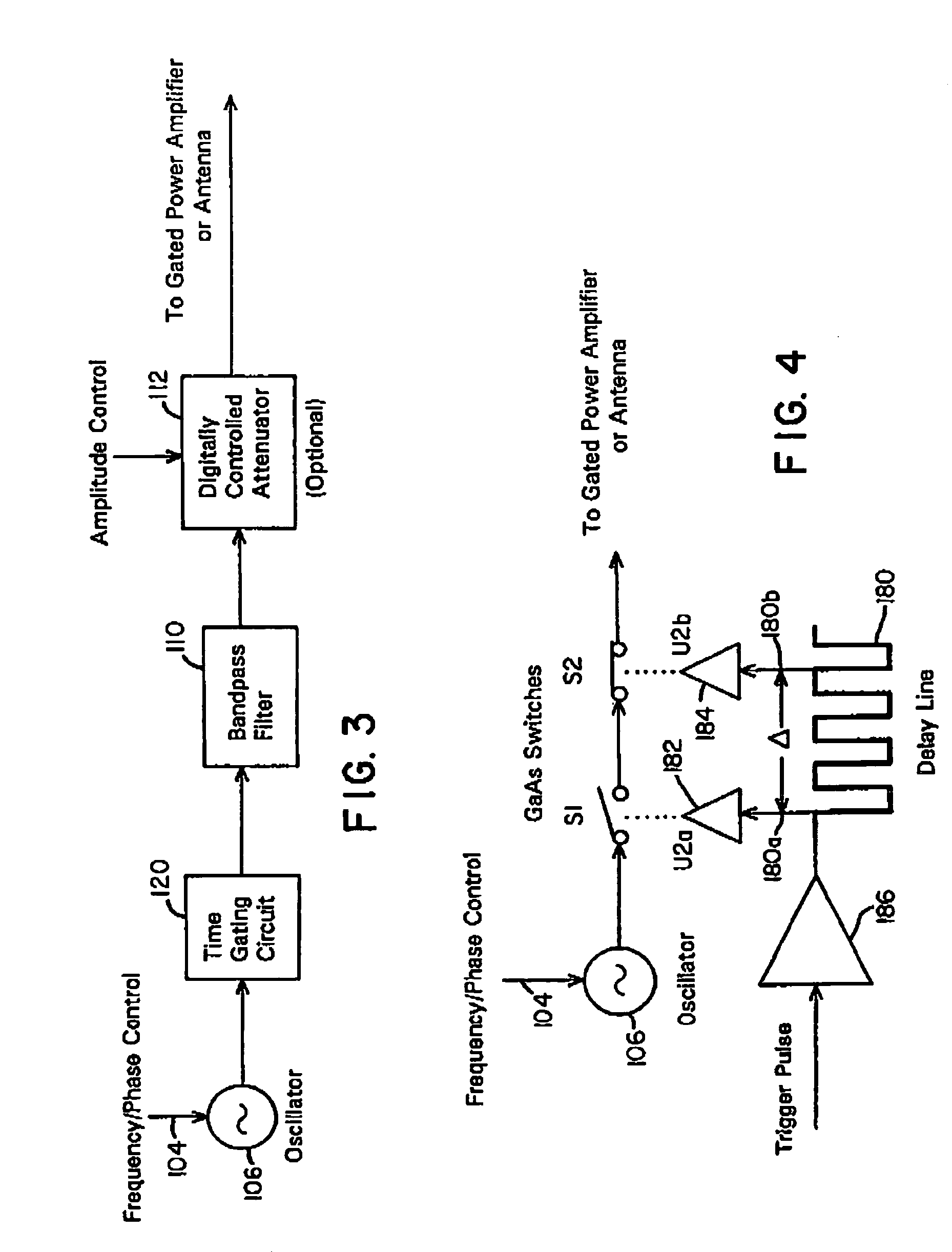
The present invention provides a breakthrough in UWB communications by generating a waveform adaptive or carrier controlled UWB signal with adjustable center frequency and bandwidth. This allows for UWB frequency hopping and adaptive bandwidth control. The invention utilizes a low-level impulse-gated oscillator and bandpass or pulse shaping filter to generate an extremely wide bandwidth pulse. A gated power amplifier is used to amplify the UWB signal and a microwave tunnel diode is utilized as a single pulse detector for high sensitivity operation at extremely high speeds. The invention also provides an UWB transmitter system with controllable spectral features, high data rates, and frequency extendibility to millimeter wave frequencies.

Problems solved by technology

To be useful for data communications, previous UWB impulse or carrier-free transmission systems have been limited to ON-OFF keying (binary amplitude shift keying ASK) or pulse position modulation (PPM) since amplitude and / or phase control of the waveform was extremely difficult or impossible to implement.
In addition, these previous systems have been fixed bandwidth and fixed frequency with no capability for frequency hopping or dynamic bandwidth control.
Output power and pulse repetition frequency (PRF) of UWB impulse transmitters have also been limited due to fundamental physical limitations of the devices used to generate the ultra-short duration pulses.
High output power impulse excitation sources such as bulk avalanche semiconductors, high voltage breakover devices, high voltage Gallium Arsenide (GaAs) thyristors, plasma diodes, stacked arrays of step recovery diodes (SRDs), etc. required hundreds to many thousands of volts for proper operation and, consequently, were limited to PRFs below a few tens of kilohertz due to increased device heating and thermal breakdown at higher PRFs.
In addition, while the individual devices were typically low cost, they often needed to be hand-selected in order to guarantee avalanche or breakdown characteristics at a particular operating voltage level.
Although these techniques proved to be reliable, the power efficiency, PRF limitations, size and complicated antenna assemblies limited performance and reproducibility.
Another significant limitation of such impulse-based UWB sources is the fact that the power level decreases with increasing frequency at a rate of approximately 12 dB per octave.
This unused energy is dissipated as heat, subjecting operating circuits to overheating and damage, and limiting the PRF or data rate at which the source can operate reliably.
Another limitation in the use of such techniques is the lack of accurate control of radiated emissions to meet regulatory requirements.
Thus, conventional UWB signal generation techniques suffer from several shortcomings:(i) high power operation can only be achieved at reduced PRFs because of device heating;(ii) practical operational frequencies are limited to well below 5 GHz due to the 12 dB per octave falloff of output impulse energy with increased frequency;(iii) impulse excitation of an antenna results in a “carrier-free” signal which would uncontrollably overlap frequencies restricted from such use, albeit with low energy densities; and(iv) modulation techniques are limited to on-off keying and pulse position modulation, with no capability for frequency hopping or for dynamic bandwidth control.
It was soon observed, however, that the Robbins TDD was subject to operating point bias drift due to temperature and power supply fluctuations.
This bias drift impacted negatively the system's overall sensitivity and increased the false alarm rate.
Since the baseband receiver was extremely broadband, with typical bandwidths of hundreds of MHz to GHz, it was found to be extremely susceptible to in-band interference and jamming since the tunnel diode circuit could not distinguish between valid and unwanted signals.
Such in-band signals caused a significant reduction in receiver sensitivity by causing the CFAR loop to back-off the sensitivity of the tunnel diode detector.
However, this anti-jam circuit proved to be ineffective in the presence of barrage (broadband) noise, jamming or interference, and / or multiple in-band CW interfences.
The broadband noise is also down converted with the signal, and no anti-jam improvement is obtained.
Moreover, to reduce the effects of the skewing, a large number of noise dwells must be detected for each data dwell detected, ultimately reducing data rates.
Unfortunately, since the BER is a very sensitive function of the tunnel diode bias level, this can result in a significant reduction in receiver sensitivity to achieve a desired BER.
While previous designs of the CFAR tunnel diode receiver have functioned reliably as an ultra wideband single pulse detector, their use in modern communication and radar applications have presented numerous drawbacks:1. The prior art designs remain susceptible to in-band interference and jamming, particularly broadband or barrage noise jamming and multiple CW interferers.2. The requirement to continuously adjust bias to the tunnel detector to maintain a given constant false alarm rate (CFAR) conventionally requires a minimum number of noise dwells to take place for each data dwell—typically thirty-two or more noise dwells for each data dwell—to achieve false alarm rates less than a few percent.
This severely restricts the maximum data rate at which a single detector can operate since data and noise dwells must operate at different time intervals.
In addition, the speed at which the tunnel diode detector can respond to sudden changes in the electromagnetic environment is limited.

Method used


Image

  • Ultra-wideband receiver and transmitter
  • Ultra-wideband receiver and transmitter
  • Ultra-wideband receiver and transmitter

Examples


first embodiment

[0132]FIG. 13 shows a simplified schematic diagram of a high speed UWB receiver according to the present invention. In FIG. 13, a received UWB pulse is input, through calibration switch S1, to a wideband, high gain RF amplifier 200. Calibration switch S1 is used to switch between an operational mode with switch S1 in the down position as shown in FIG. 13, and a calibration mode with switch S1 in the up position connecting the input of high gain RF amplifier 200 to ground through impedance matching resistor 208, which in this embodiment is 50 ohms. In the preferred mode, calibration switch S1 is switched only once after power-up and is activated by a programmable logic device or microprocessor 210.

Receiver ‘Operational Mode’

[0133]With calibration switch S1 in the operation mode position, after RF amplification, the UWB pulse is input to voltage variable attenuator (VVA) 202, whose primary function is to provide high speed, adaptive dynamic range extension. The adaptive dynamic range ...

second embodiment

[0177]This problem can be overcome by the present invention as shown in FIG. 17, which utilizes two tunnel diode detectors to allow for parallel data and noise dwells, thus allowing for even higher speed operation than that allowed by the single tunnel diode detector embodiment shown in FIG. 13. In this embodiment, all dwells are both data dwells and noise dwells.

[0178]In an UWB receiver utilizing a single tunnel diode detector, the maximum number of noise dwells that can occur for each data dwell is reduced as the data rate increases. The UWB receiver having two tunnel diode detectors—one for the detection of energy with respect to a noise threshold and the other for the detection of energy with respect to a data threshold, e.g. as shown in FIG. 17, has certain advantages over a single tunnel diode 222 design switched between a noise threshold and a data threshold as shown in FIG. 13. For instance, in a single tunnel diode design, as the data rate increases, the time between data d...


PUM


Abstract

A waveform-adaptive ultra-wideband (UWB) transmitter and noise-tracking UWB receiver for use in communications, object detection and radar applications. In one embodiment, the output of an oscillator is gated by a low-level impulse generator either directly or through an optional filter. In a special case of that embodiment wherein the oscillator is zero frequency and outputs a DC bias, a low-level impulse generator impulse-excites a bandpass filter to produce an UWB signal having an adjustable center frequency and desired bandwidth based on a characteristic of the filter. In another embodiment, the low-level impulse signal is approximated by a time-gated continuous-wave oscillator to produce an extremely wide bandwidth pulse with deterministic center frequency and bandwidth characteristics. The low-level impulse signal can be generated digitally. The UWB signal may be modulated to carry data, or may be used in object detection or ranging applications. The power amplifier may be gated to provide a power-efficient UWB transmitter. The UWB transmitter exhibits well defined and controllable spectral characteristics. The UWB transmitter is capable of extremely high pulse repetition frequencies (PRFs) and data rates in the hundreds of megabits per second or more, frequency agility on a pulse-to-pulse basis allowing frequency hopping if desired, and extensibility from below HF to millimeter wave frequencies.

Description

CROSS-REFERENCE TO RELATED APPLICATIONS[0001]This application combines the transmitter-receiver disclosures and is a continuation-in-part of commonly-owned U.S. patent application Ser. Nos. 08 / 857,836 and 08 / 872,729 filed May 16, 1997 and Jun. 11, 1997, respectively, by the same inventors hereof (now U.S. Pat. Nos. 6,026,125 and 5,901,172, respectively). The subject matter of each of said applications is incorporated herein.[0002]This application is also related to commonly-owned U.S. application Ser. No. 09 / 118,919 filed Jul. 20, 1998 (now U.S. Pat. No. 6,239,741), also incorporated herein.BACKGROUND OF THE INVENTION[0003]1. Field of the Invention[0004]This invention relates to the field of ultra-wideband communication systems. More particularly, it relates to the controlled transmission and reception of ultra-wideband electromagnetic pulses.[0005]2. Background of Related Art[0006]Ultra-wideband (UWB) systems, both for radar and communications applications, have historically utiliz...

Claims


Application Information

Patent Timeline
Patent Type & Authority Patents(United States)
IPC IPC(8): H04L27/04H03K9/00
CPCH04B1/71635H04B1/71637H04B1/7172H04B1/7174H04B2001/6908
Inventor LARRICK, J. FREDERICKFONTANA, ROBERT J.
Owner ZEBRA TECH CORP
Learn More