Semiconductor memory device

a memory device and semiconductor technology, applied in the direction of digital storage, instruments, power supply for data processing, etc., can solve the problems of increasing the consumption of pseudo-sram power, leakage of current, and inability to achieve effective reduction to stand-by state, so as to achieve the effect of reducing the consumption of curren

Inactive Publication Date: 2006-12-05
RENESAS ELECTRONICS CORP
View PDF1 Cites 7 Cited by
  • Summary
  • Abstract
  • Description
  • Claims
  • Application Information

AI Technical Summary

Benefits of technology

[0016]In accordance with this configuration, in the interval of time period between the refresh operations to be executed independently from the operating modes, the leak path of the system of circuits associated with the refresh operations is broken down, so that a consumption of current of this system of circuits is limited to a consumption of current generated in periods of time of actual fresh operations. The time of the refresh operation is sufficiently shorter than the interval of time period between the refresh operations and a refresh cycle time, for which reason the consumption of current of the system of circuits associated with the refresh operations is effectively reduced. In addition to this leak breaking means, another leak breaking means may be used for breaking down always a leakage of current of another system of circuits which remain in an inactive state in a stand-by mode, for the purpose of a further reduction to the consumption of current.
[0025]In accordance with this configuration, it is possible to reduce the power voltage without reducing the operating speed of the system of circuits associated with the refresh operations. Thus, a further reduction to the power consumption through the reduction of the power voltage is available without reducing the operating speed.
[0027]In accordance with this configuration, a consumption of current by the circuit acting as the non-critical path can be reduced without reducing the operating speed of the circuit acting as the critical path. Accordingly, the consumption of current can be effectively reduced without dropping the operating speed apparently.
[0029]In accordance with this configuration, even if the chip select signal is toggled in a short time period, while the internal chip select signal is maintained in the active state. Accordingly, the system of circuits controlled by this internal chip select signal shows no unnecessary operations for avoiding unnecessary operating currents.

Problems solved by technology

This causes increasing the consumption of power of the pseudo-SRAM.
Particularly, there is a problem with a remarkable leakage of current as an unnecessary consumption of current in an interval of time period (between refresh operations) which is much longer than a time necessary for cyclic executions of refresh operations.
The above-described prior art is applicable to a system of circuits inactivated in the stand-by mode but not applicable to another system of circuits which may be activated in the stand-by mode such as the system of circuits associated with the refresh in the pseudo-SRAM, wherein any effective reduction to the stand-by state can not be obtained.

Method used


Image

  • Semiconductor memory device
  • Semiconductor memory device
  • Semiconductor memory device

Examples


first embodiment

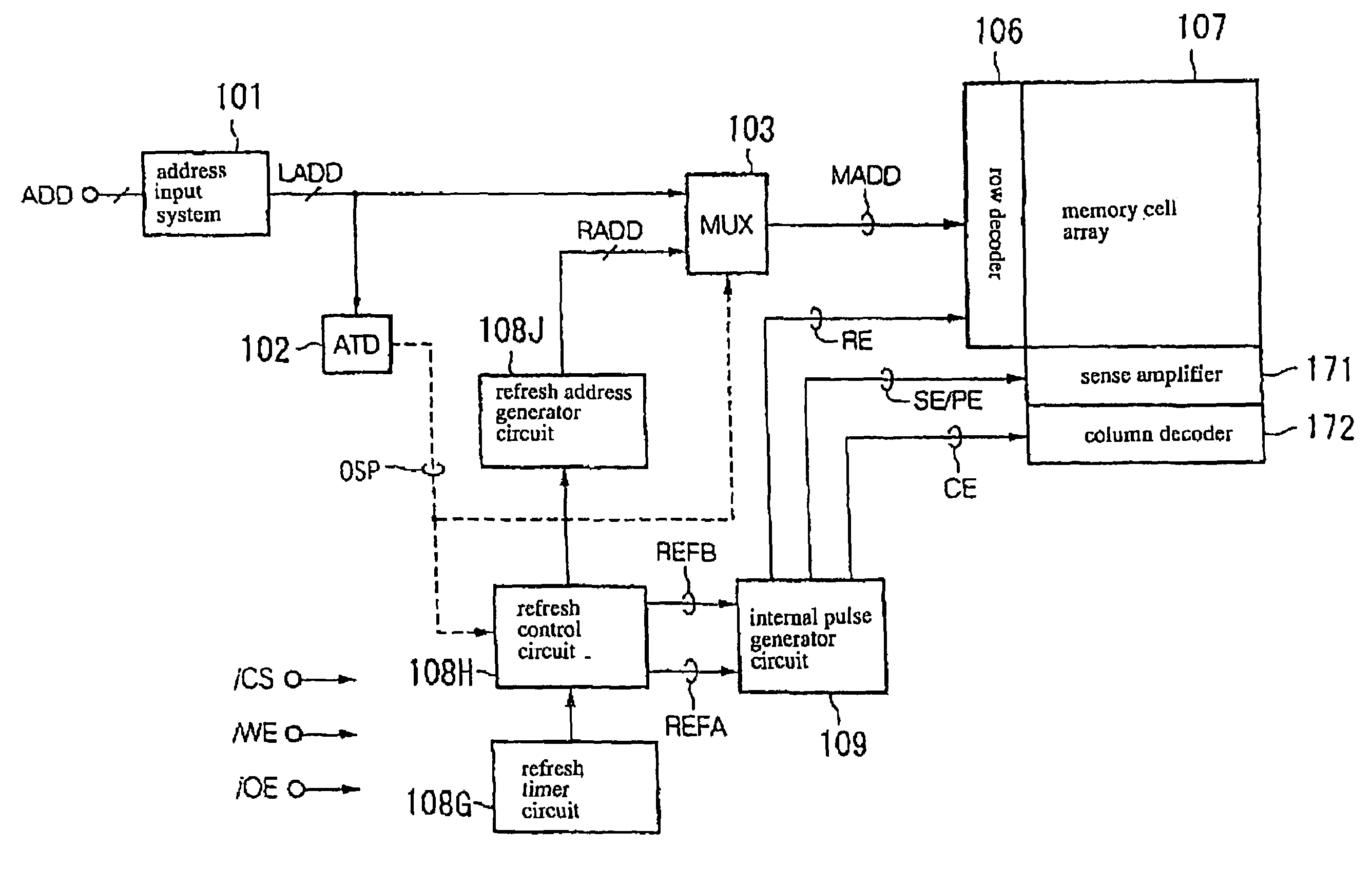
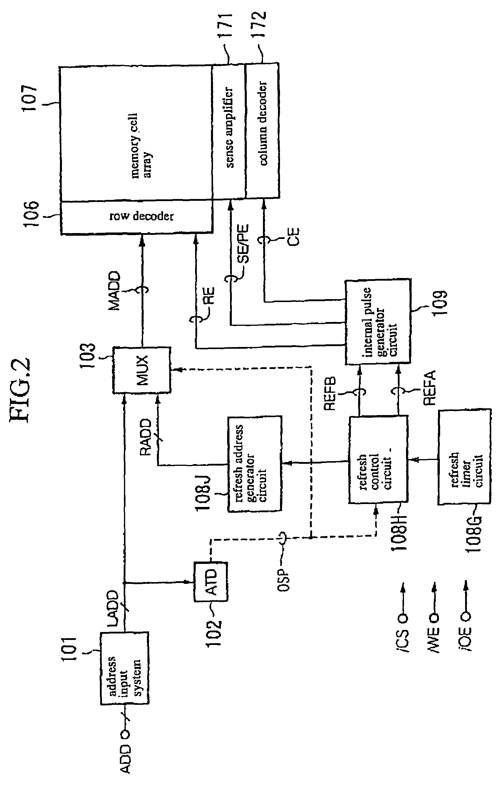
[0042]In accordance with this first embodiment, a semiconductor memory device comprises a pseudo-SRAM having a basic configuration of DRAM and being configured to allow an external asynchronous access, wherein the semiconductor memory device includes a refresh circuit system for automatically refreshing data stored in memory cells with timings matched over plural operation modes. The semiconductor memory device also includes a leak breaking means for breaking a leak path between the above refresh circuit system and either a power source or a ground in an interval of time period between the refresh operations for the purpose of reducing the consumption of current.

[0043]The following descriptions will be made for basic configuration and operation related to the refresh operations before describing characteristic configuration and operation of reducing the leakage of current of the system of circuits associated with the refresh operations.

(1) Basic Configuration and Operation in View o...

second embodiment

[0115]The second embodiment of the present invention will be described hereinafter.

[0116]In accordance with this second embodiment, in addition to the above-described configuration of the first embodiment, a gate threshold voltage of transistors forming a critical path is set lower than a gate threshold voltage of transistors forming a non-critical path. FIG. 9 shows an example of the characteristic configuration of the semiconductor memory device in accordance with the second embodiment.

[0117]This example shown in the drawing includes memory cells and those peripheral circuits. In this drawing, a MOS transistor encompassed by a circle mark is a transistor having a high gate threshold voltage. The code MC represents memory cells aligned in matrix and being connected bit lines B, / B running in a column direction, and word lines WL running in a row direction. Each of the memory cells MC comprises a single transistor and a single capacitor, wherein one electrode of the capacitor is fix...

third embodiment

[0138]The third embodiment will be described hereinafter.

[0139]In his third embodiment, a power circuit in the cell array block 1 shown in FIG. 4 in the above-described first embodiment is controlled by the internal chip select signal CSI in order to reduce the leakage of current of the cell array block 1.

[0140]The cell array block 1 has a large number of drivers for selecting memory cells for executing the refresh operations, for which reason the cell array block 1 is involved into the system of circuits associated with the refresh operations.

[0141]As shown in FIG. 11, in this third embodiment, a power supply circuit for supplying the power HVD to the above-described driver 300 shown in FIG. 9 comprises a diode 401, a p-channel transistor 402, and a CMOS-configured inverter 403. A gate threshold voltage of MOS transistors forming the p-channel transistor 402 and the inverter 403 is set higher than a gate threshold voltage of the MOS transistors forming the driver 300. A ground supp...


PUM


Abstract

A semiconductor memory device is provided which effectively reduces a consumption of current of a system of circuits associated with refresh operations. A control signal circuit 2 controls n-channel transistors 3C, 4B to be in an OFF-state based on an internal chip select signal SCI in an interval time period between the refresh operations, wherein the n-channel transistors 3C, 4B are connected between the system of circuits associated with refresh operations (an internal voltage-down circuit 3 and a boost circuit 4) and the ground, so as to break down a leak path of the system of circuits associated with refresh operations for reducing the leakage of current. At a timing of starting the refresh operation by triggering a timer, the internal chip select signal SCI is transitioned to a high level for supplying a ground voltage to the internal voltage-down circuit 3 and the boost circuit 4.

Description

CROSS-REFERENCE TO RELATED APPLICATIONS[0001]The present application is a divisional of U.S. patent application Ser. No. 10 / 479,729, filed Dec. 5, 2003, now U.S. Pat. No. 6,922,371, which is a continuation of PCT / JP02 / 05169 filed May 28, 2002.TECHNICAL FIELD[0002]The present invention relates to a semiconductor memory device which needs a refresh operation for stored data, and more particularly to a technique for reducing a consumption of current by a system of circuits associated with refresh operation.BACKGROUND ART[0003]A pseudo-SRAM has conventionally been utilized for a portable device, wherein the pseudo-SRAM has both an advantage of a DRAM (Dynamic Random Access Memory) suitable for a large capacity and another advantage of an SRAM (Static Random Access Memory) making it easy to design timings. In the field of this type, requests for scaling down the device and for improving long life-time of a battery have been on the increase year by year. The pseudo-SRAM comprises a basic ...

Claims


Application Information

Patent Timeline
Patent Type & Authority Patents(United States)
IPC IPC(8): G11C5/14G06F1/32G11C11/403G11C11/406G11C11/407G11C11/4074
CPCG11C11/406G11C11/40615G11C11/4074G11C2207/2227G11C2211/4067G11C11/34
Inventor TAKAHASHI, HIROYUKINAKAGAWA, ATSUSHIINABA, HIDEO
Owner RENESAS ELECTRONICS CORP
Why Eureka
Try Eureka