Real time analytical monitor for soft defects on reticle during reticle inspection

a technology of soft defects and real-time analytical monitors, applied in the field of semiconductor processing, can solve the problems of difficult determination based solely on knowledge of the existence of defects, and achieve the effect of facilitating correct decisions, large defects, and high precision

Active Publication Date: 2006-06-27
GLOBALFOUNDRIES US INC
View PDF7 Cites 25 Cited by
  • Summary
  • Abstract
  • Description
  • Claims
  • Application Information

AI Technical Summary

Benefits of technology

[0010]The present invention provides for systems and methods for analyzing soft defects on a reticle during reticle defect inspection in real time without the need for a defect navigation system. If the reticle is associated with a pellicle, the present invention can detect and analyze defects in a non-pellicle region of the reticle. More specifically, the present invention provides for reticle soft defect chemical analysis via utilizing a chemical analysis component to analyze detected soft defects on a reticle in conjunction with a Focused Ion Beam (FIB). The FIB produces a finely focused ion beam, which can be directed at any particular spot on a reticle with high precision and can be rastered over an area of arbitrary size and shape.
[0011]The multi-functionality of the FIB in conjunction with a composition analysis tool is especially suited to semiconductor production because it permits a defect both to be imaged and manipulated. This is particularly important because, while not all reticle defects will adversely affect the finished device, it is difficult to make such a determination based solely upon knowledge of the existence of the defect. Rather, analysis of the composition of the defect facilitates a correct decision as to whether time should be sacrificed to unload a defective reticle and discard a recent batch of product or whether manufacture can continue despite a benign defect. Thus, the present invention permits analytical capability in reticle defect inspection without the need for a separate defect identification and navigation system. More specifically, the invention can determine whether sulfur, phosphorus, and / or amine(s) are present in a soft defect, which can result in adder defects over time.
[0012]According to one aspect of the present invention, chemical analysis of a soft defect can be performed to detect any extant sulfur signature in the defect. Although the present invention is described largely with regard to detecting sulfur signatures, it is to be understood that the invention can detect signatures associated with phosphorus, amine groups, or any other chemical compound capable of causing adder defect growth on a reticle. Scanning Electron Microscopy (SEM) can be utilized to image the reticle at a defect location. A FIB can be employed with a low beam current to scan and / or image reticle defects, or with a high beam current to cut a cross-section of the defect. The FIB is capable of cutting from either a top layer or a bottom layer. The utilization of the FIB to remove a thin layer of material from a defect ensures that the defect surface is clear of contaminants. Upon discovery of a soft defect, an Electron Spectroscopy Chemical Analysis (ESCA) beam can be employed to determine the material composition of the soft defect. The information acquired during analysis can be fed to a processor for determination of the chemical composition of the defect. According to a particular aspect of the invention, the ESCA specifically analyzes the defect for a sulfur signature. If a sulfur signature is found, the system can alert a user to remove the reticle for cleaning and / or repair. Additionally, the system can inform a user of the presence of sulfur on the reticle and permit the user to make a determination of whether the reticle requires cleaning and / or repair.
[0013]According to another aspect of the invention, a Fourier Transform Infrared Spectroscopy (FTIR) beam can be employed to determine the chemical composition of a soft defect in the event that the defect is larger than a predetermined value, for example greater than 100 microns in diameter. Larger defects can ultimately be removed using conventional methods. However, the presence of sulfur, phosphorus, etc., signatures is highly indicative of the presence of such elements and / or compounds between the reticle and pellicle. Knowledge of such a contaminant(s) between a pellicle and a reticle can facilitate making a more educated decision regarding whether to remove a reticle from a stepper for cleaning and / or rejection, which in turn permits resources to be expended more wisely.

Problems solved by technology

This is particularly important because, while not all reticle defects will adversely affect the finished device, it is difficult to make such a determination based solely upon knowledge of the existence of the defect.

Method used


Image

  • Real time analytical monitor for soft defects on reticle during reticle inspection
  • Real time analytical monitor for soft defects on reticle during reticle inspection
  • Real time analytical monitor for soft defects on reticle during reticle inspection

Examples


Embodiment Construction

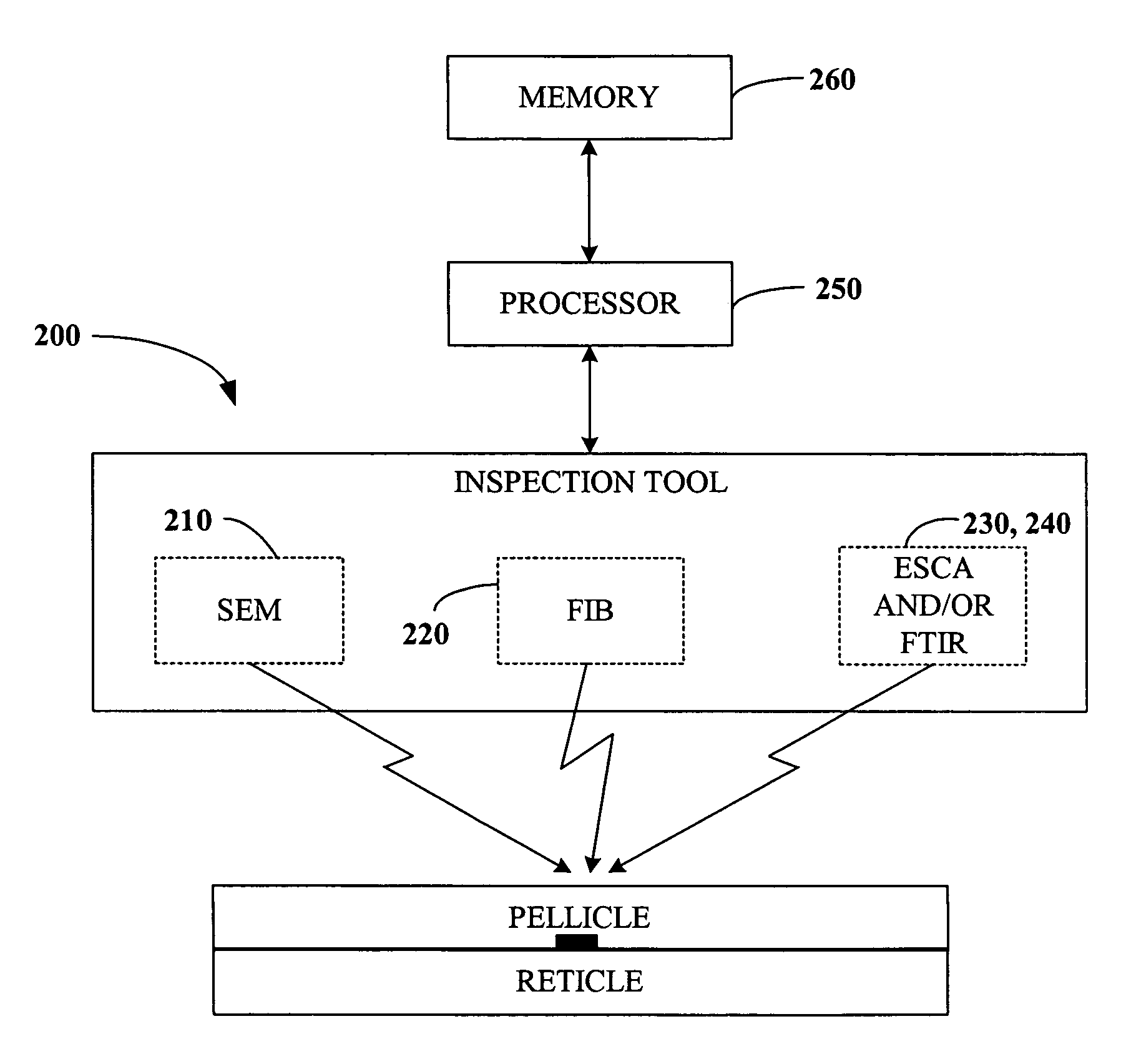
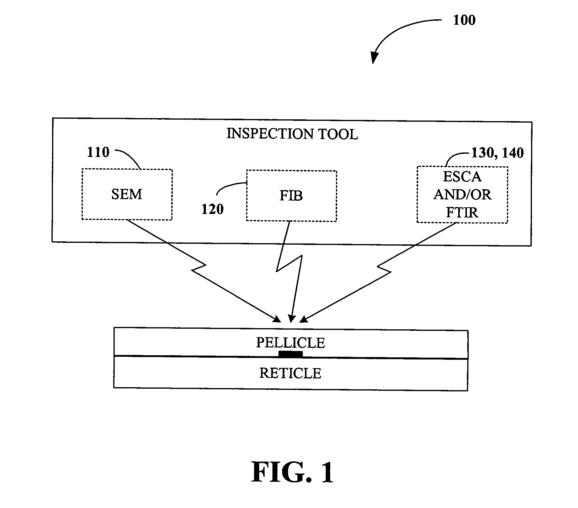
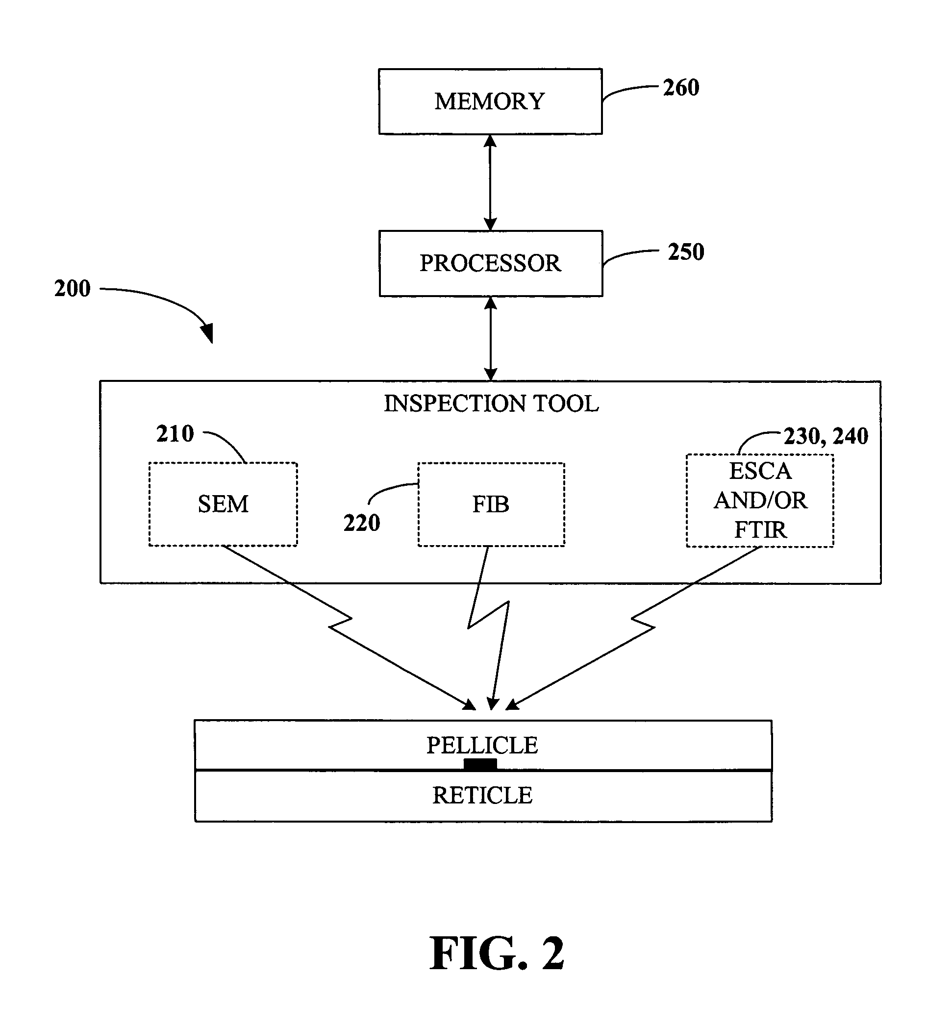
[0030]The present invention will now be described with reference to the drawings, wherein like reference numerals are used to refer to like elements throughout. The present invention will be described with reference to a system for inspecting and / or correcting reticle defects in real time. It should be understood that the description of these exemplary aspects are merely illustrative and that they should not be taken in a limiting sense.

[0031]The term “component” refers to a computer-related entity, either hardware, a combination of hardware and software, software, or software in execution. For example, a component can be a process running on a processor, a processor, an object, an executable, a thread of execution, a program and a computer. By way of illustration, both an application running on a server and the server can be components. A component can reside in one physical location (e.g., in one computer) and / or can be distributed between two or more cooperating locations (e.g., ...


PUM

PropertyMeasurementUnit
diameteraaaaaaaaaa
speedaaaaaaaaaa
speedaaaaaaaaaa

Abstract

The present invention generally relates to semiconductor processing, and in particular to methods and systems for analyzing photolithographic reticle defects that include detecting soft defects on a reticle and analyzing the material composition of the defects for a particular chemical signature. Specifically, the present invention scans and images a soft defect via an optical inspection scan of a reticle, mills the defect using a Focused Ion Beam, and analyzes the defect for signatures using Electron Spectroscopy for Chemical Analysis and / or Fourier Transform Infrared Spectroscopy. The present invention thus provides for real-time analysis of the chemical composition of a soft defect on a reticle without the need for a defect identification navigation system. According to an aspect of the present invention, reticle defects can be monitored without removal of a pellicle, thus facilitating increased throughput and decreased cost in reticle repair and / or cleaning. According to another aspect of the invention, signatures occurring in trace amounts can be removed via employing a Focused Ion Beam in a non-reactive gas environment.

Description

TECHNICAL FIELD[0001]The present invention generally relates to semiconductor processing, and in particular to methods and systems that analyze photolithographic reticle defects via detecting soft defects on a reticle and determining the material composition of the defects.BACKGROUND OF THE INVENTION[0002]As semiconductor trends continue toward decreased size and increased packaging density, every aspect of semiconductor fabrication processes is scrutinized in an attempt to maximize efficiency in semiconductor fabrication and throughput. Many factors contribute to fabrication of a semiconductor. For example, at least one photolithographic process can be used during fabrication of a semiconductor. This particular factor in fabrication processes is highly scrutinized by the semiconductor industry in order to improve packaging density and precision in semiconductor structure.[0003]Lithography is a process in semiconductor fabrication that generally relates to transfer of patterns betwe...

Claims


Application Information

Patent Timeline
Patent Type & Authority Patents(United States)
IPC IPC(8): G01B5/28G06K9/00G03F1/14G01B5/00G03F1/00
CPCG01N21/3563G01N21/95692G03F1/84G06T7/0004G03F1/82G01N2021/3595G01N2021/95676G03F1/62H01J2237/31744G06T2207/30148H01J2237/304
Inventor PHAN, KHOISINGH, BHANWARRANGARAJAN, BHARATH
Owner GLOBALFOUNDRIES US INC
Why Eureka
Try Eureka