Soldering flux, solder paste and method of soldering

Inactive Publication Date: 2005-07-12
TDK CORPARATION
View PDF20 Cites 30 Cited by
  • Summary
  • Abstract
  • Description
  • Claims
  • Application Information

AI Technical Summary

Benefits of technology

[0015]It is an object of the present invention to provide a soldering flux, a soldering paste and a soldering method that achieve a sufficient degree of bonding strength while allowing higher mounting density; further miniaturization of components and a reduction in the pitch at which components are set.
[0016]It is a further object of the present invention to provide a soldering flux, a soldering paste and a soldering method that prevent components from becoming lifted off or falling off with a high degree of reliability without having to ensure a sufficient difference between the melting points of the solders used at the two surfaces of a double-sided installation type component mounting board.
[0017]It is a still further object of the present invention to provide an electronic component device, an electronic circuit module and an electronic circuit apparatus that may be manufactured at low production costs without requiring a flux washing process.

Problems solved by technology

Thus, it is difficult to ensure a sufficient soldering strength even today.
Since it is expected that higher density at the mounting board, further miniaturization of components and a smaller pitch between individual components will be pursued with increasing vigor in the future, it will become even more difficult to support this technical trend with the means for assuring the bonding strength in the related art that achieves the required bonding strength simply by allowing the solder joint to be formed over a large enough area.
However, since the bonding area of the fillet portion itself is bound to be reduced in high-density mounting, the fillet portion cannot readily contribute to an increase in the bonding strength.
However, no Pb-free solder composition with a high melting point comparable to that of a high-temperature solder in the prior art has been put into practical use to date.
The main obstacle is that the melting point of Pb-free solder itself is approximately 220° C. that is higher than the melting point of a eutectic solder by as much as 40° C. and thus, no effective alternative to Pb has been discovered.
Consequently, the issue of insufficient difference between the melting points of the solders used on the two sides of a double-sided installation type component mounting board is yet to be addressed, and the problem of components becoming lifted off or falling off when they are mounted onto the component mounting board is still common.
However, if there is any residual flux present when the sealant is injected, the flux prevents the sealant from reaching the interface between the semiconductor chips and the board in sufficient quantity and thus, the sealant fails to achieve its full bonding strength.
Moreover, when a combination of a ceramic substrate and an organic resin substrate is adopted to constitute the chip mounting board and the motherboard respectively to manufacture an electronic circuit apparatus by mounting an electronic circuit module obtained through the process described above onto the motherboard, the contraction stress tends to concentrate in the solder joint to result in cracks to occur readily in the solder joint to result in a reduction in the durability of the joints due to the difference between the coefficients of thermal expansion of the ceramic board and the organic resin board, as proven in thermal shock tests and the like conducted after the electronic circuit module is mounted.
While it would be desirable to inject a sealant in order to improve the strength of the solder joint for this reason, it would lead to a considerable increase in the production cost to implement a flux washing process and a sealant injection process on the entire motherboard, and thus, the sealant is not injected in reality.

Method used


Image

  • Soldering flux, solder paste and method of soldering
  • Soldering flux, solder paste and method of soldering
  • Soldering flux, solder paste and method of soldering

Examples


embodiment 1

[0064]Bisphenol A was used to constitute the thermo-setting resin and an anhydride of carboxylic acid was used as a hardening agent. The mixing ratio of the thermo-setting resin and the hardening agent was set at 1:1 by weight. In addition, a required degree of viscosity was assured by mixing in small quantities of a solvent and a thixotropic agent.

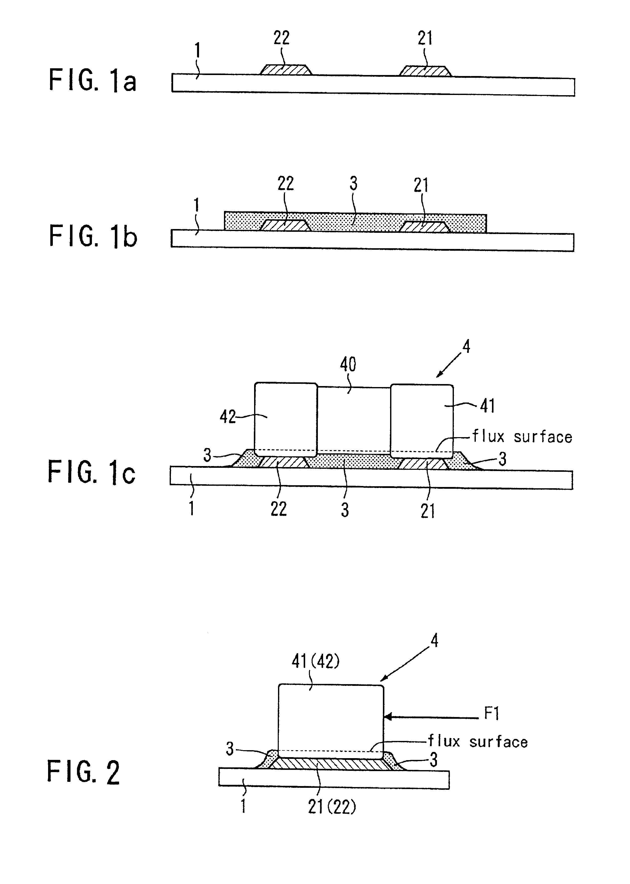
[0065]A flux 3 prepared by adopting the composition described above was applied (see FIG. 1b) onto a component mounting board 1 (see FIG. 1a) upon which solder bumps 21 and 22 had been deposited in advance. Next, as illustrated and FIG. 1c, an electronic component 4 achieved as a 1 mm (length)×0.5 mm (width) chip was mounted. The electronic component 4 having terminal electrodes 41 and 42 provided at the two ends of a base body 40 to face opposite each other was mounted onto the component mounting board 1 so as to set the terminal electrodes 41 and 42 on the solder bumps 21 and 22 respectively. The component mounting board 1 having been m...

embodiment 2

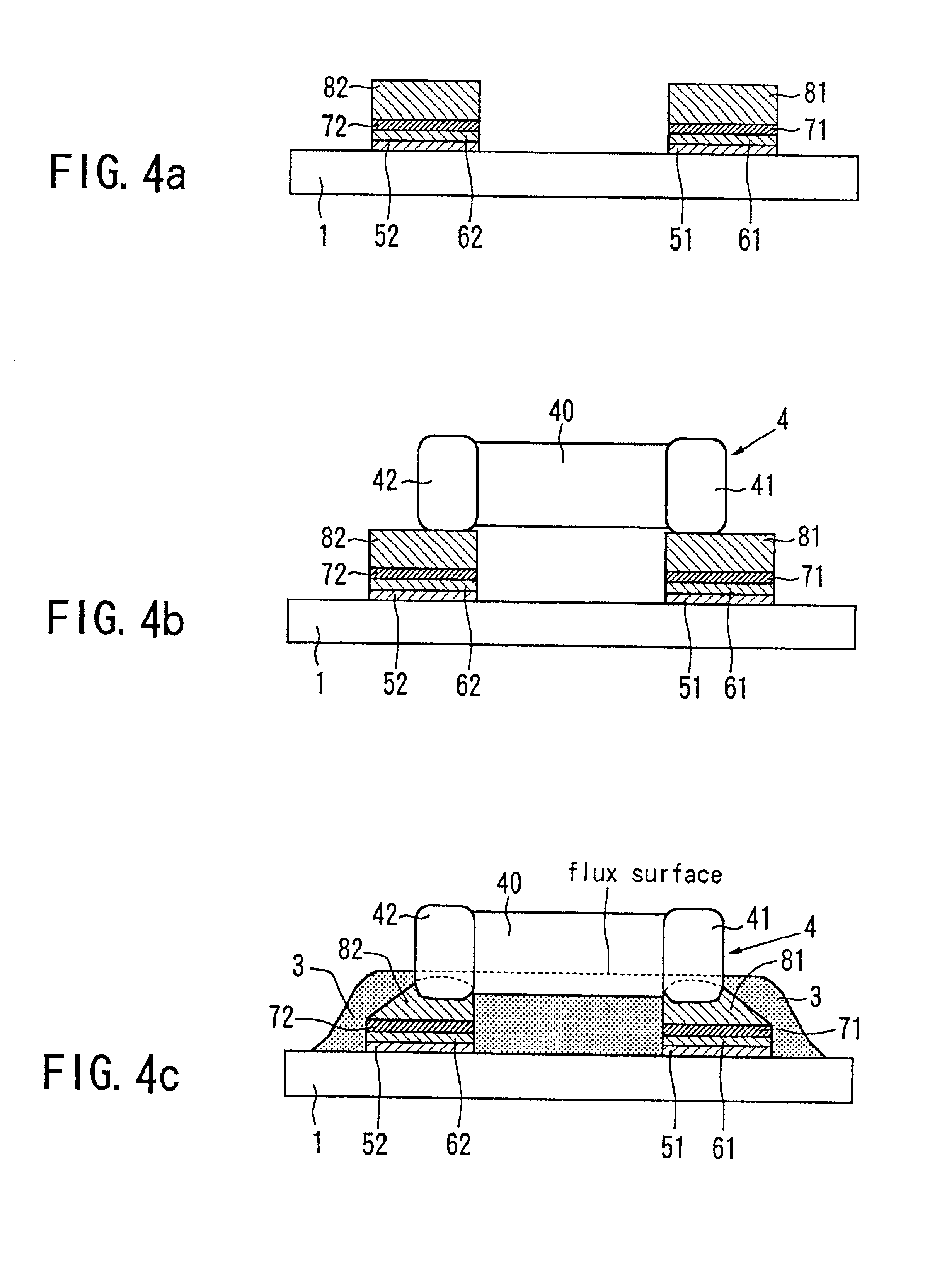
[0069]A soldering paste was prepared by mixing the flux prepared in embodiment 1 with soldering powder. The quantity of the flux that was mixed relative to the quantity of the soldering powder was set at 10 wt %. A chip component was soldered onto a component mounting board using this soldering paste. FIGS. 4a through 4c present partial cross-sectional views, showing the component mounting board in detail and the soldering process through which the chip component was soldered onto the component mounting board. The component mounting board 1 included two lands formed by sequentially laminating a Cu film 51 (52), an Ni film 61 (62) and an Au film 71 (72).

[0070]The soldering paste 81 (82) according to the present invention was applied onto each land at the component mounting board 1 (see FIG. 4a). The soldering paste 81 (82) was applied through a printing process implemented by using a metal mask having a 100 μm thickness. The dimensions of the opening at the metal mask were set to 0.5...

embodiment 3

[0077]A soldering paste was prepared by mixing the flux prepared in embodiment 1 with soldering powder. The quantity of the flux that was mixed relative to the quantity of the soldering powder was increased to 20 to 45 wt %.

[0078]An electronic component 4 was soldered onto a component mounting board 1 using this soldering paste as illustrated in FIG. 7. To explain in more specific terms in reference to FIG. 7, the component mounting board 1 included two lands formed by sequentially laminating a Cu film 51 (52), an Ni film 61 (62) and an Au film 71 (72) (see FIG. 7a).

[0079]The soldering paste 81 (82) according to the present invention was applied onto each land at the component mounting board 1 (see FIG. 7a). The soldering paste 81 (82) was applied through a printing process implemented by using a metal mask having a 100 μtm thickness. The dimensions of the opening at the metal mask were set to 0.5 mm×0.3 mm to match the dimensions of the lands on which the electronic component 4 was...


PUM

PropertyMeasurementUnit
Temperatureaaaaaaaaaa

Abstract

The present invention relates to a soldering flux, a soldering paste and a soldering method that achieve a sufficient degree of bonding strength even when components are mounted at a higher density, components are further miniaturized or components are mounted with a smaller pitch. A flux 3 contains an adhesive resin and a hardening agent. This flux or a soldering paste containing the flux is applied onto a component mounting board 1, and then, an electronic component 4 is mounted and soldered onto the component mounting board 1.

Description

BACKGROUND OF THE INVENTION[0001]1. Field of the Invention[0002]The present invention relates to a soldering flux, soldering paste, an electronic component device, an electronic circuit module, an electronic circuit apparatus and a soldering method.[0003]2. Description of the Prior Art[0004]A flux is used to solder a component onto a component mounting board in the known art. The main function of the flux is to improve the wettability of the solder by removing the oxide film formed at a metal conductor provided at the component mounting board and also at the surface of the metal to be soldered at the component. Among fluxes used in the related art, those containing rosin as the primary constituent are the best known. Rosin contains a carboxylic acid such as abietic acid or levopimaric acid, and the carboxyl group acts to remove the oxide film at the surface of the metal to be soldered.[0005]Various additives such as solvents, plasticizers and thixotropic agents are normally mixed in...

Claims


Application Information

Patent Timeline
IPC IPC(8): B23K35/36H05K3/30H05K3/34B23K35/02
CPCB23K35/3613B23K35/3618H05K3/305H05K3/3489B23K35/025H05K3/3484H05K2201/10977H05K3/3485Y02P70/50
Inventor TAKAYA, MINORUABE, HISAYUKI
Owner TDK CORPARATION
Why Eureka
Try Eureka