Phase-width balanced alternating phase shift mask design

a phase shift mask and phase width balance technology, applied in the field of photolithographic methods, can solve the problems of limited exposure system resolution, failure of process, undesired shadows in projected images, etc., and achieve the effect of satisfying patterning

Inactive Publication Date: 2005-05-31
IBM CORP
View PDF13 Cites 26 Cited by
  • Summary
  • Abstract
  • Description
  • Claims
  • Application Information

AI Technical Summary

Benefits of technology

[0080]The present invention addresses the above-described need by providing a method for optimizing the design of an alternating phase shifted mask (altPSM) by selecting phase shapes that suitable have p

Problems solved by technology

The resolution of an exposure system is limited by the contrast of the projected image, that is, the intensity difference between adjacent light and dark image features.
Since recessed regions on the photo-mask can be fabricated only in closed polygons rather than individual edges, destructive interference of light across phase region edges which do not line up with desired circuit patterns, causes undesired shadows in the projected image.
A problem arises when the dimensions of the critical feature of a device falls below a narrow dimension which may lead to problems such as delamination of narrow strips on a mask used to expose the resist patterns using the altPSM method leading to failure of the process.
A

Method used


Image

  • Phase-width balanced alternating phase shift mask design
  • Phase-width balanced alternating phase shift mask design
  • Phase-width balanced alternating phase shift mask design

Examples


first embodiment

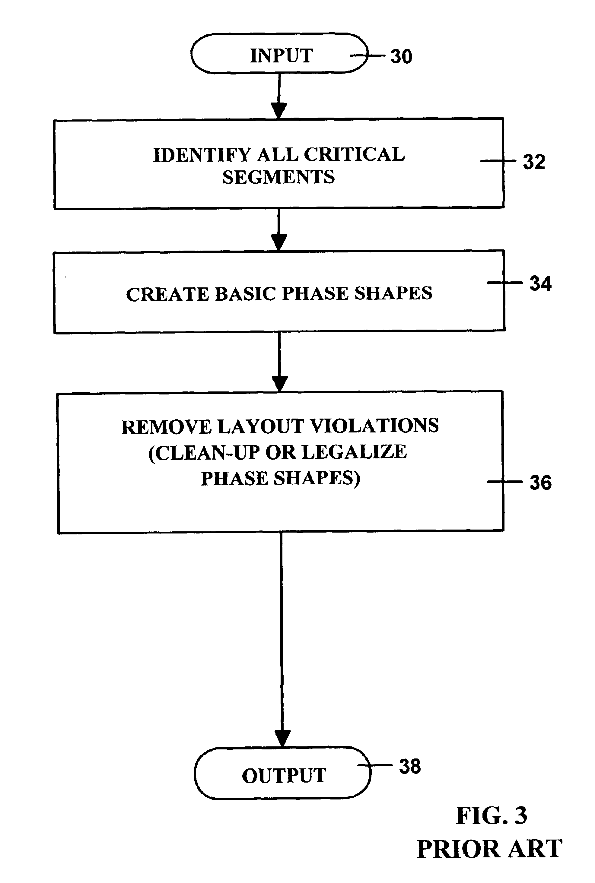
[0096]FIG. 8 is a flow chart illustrating the method of this invention for selectively adjusting the width of phase regions to locally re-balance the phase widths. The program shown in FIG. 8 begins in step 40 which leads to step 42 of identifying the critical segments of the phase shapes in the transistors layouts which are the thin legs VA / VB / VC shown in FIG. 5

[0097]In step 44, the system creates basic phase shapes withe phase regions 12A / 14A for leg VA, phase regions 14B / 12B for leg VB and phase regions 14C / 12C for leg VC.

[0098]Next in the program proceeds along line 45 to step 46 to remove layout violations, i.e. clean up or legalize the phase shapes. For example in FIG. 5, the narrow phase shapes 14A / 14B are too close to satisfy the criterion which states that the remaining thin slivers of the opaque mask may not fall below a minimum width. The result of this step is the merger of the narrow 180° phase shapes 14A / 14B in FIG. 5 into the wider 180° phase shape 24 in FIG. 6.

[0099]...

second embodiment

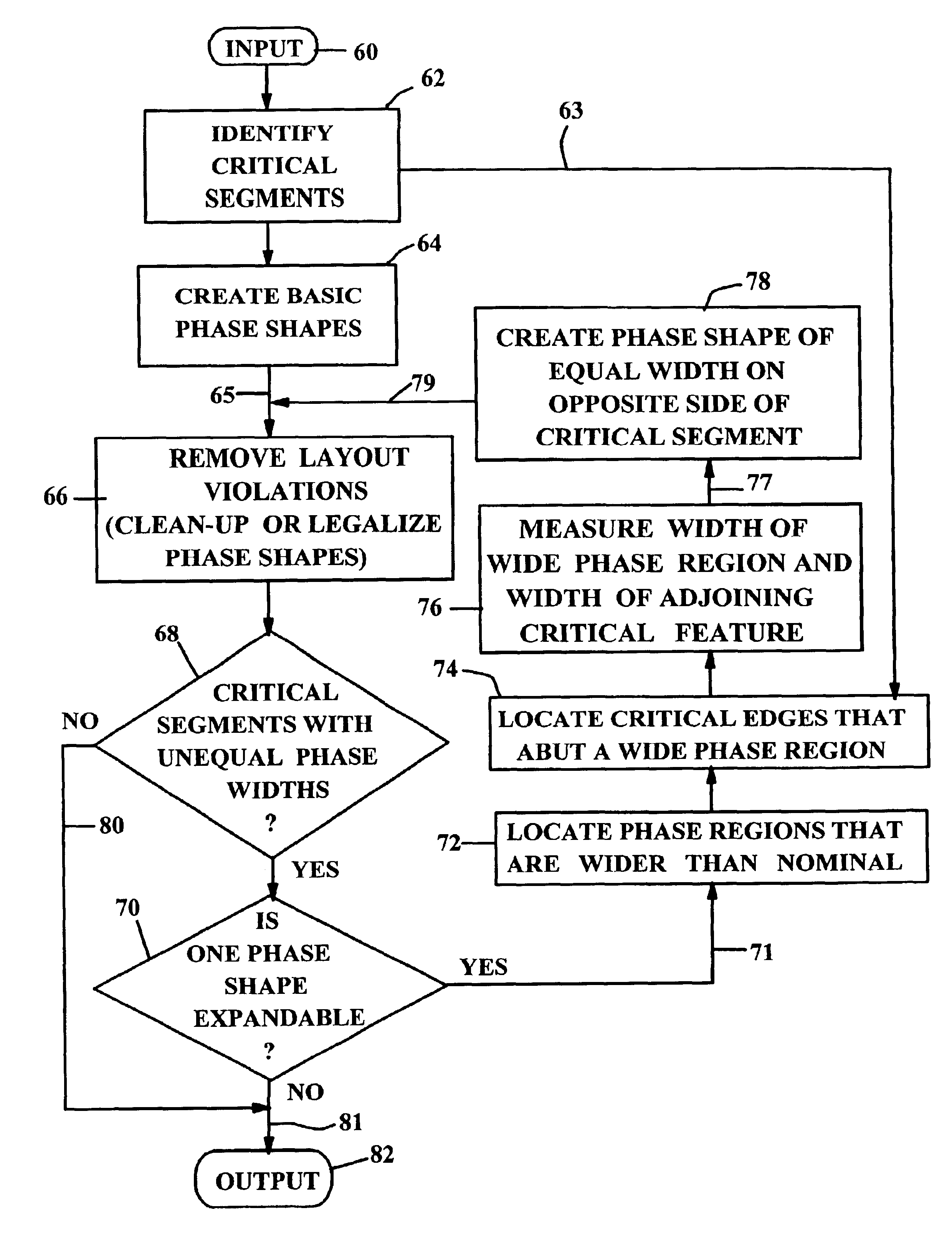
[0103]FIG. 9 shows the flowchart of the method of this invention which is a modification of the method of FIG. 8. The program shown in FIG. 8 begins with step 60 which leads to step 62 of identifying the critical segments of the phase shapes in the transistors layouts which are the thin legs VA / VB / VC shown in FIG. 5. Step 62 provides an output to step 64 as well as providing an output on line 63 to step 74, which is discussed below.

[0104]Next in step 64, the system creates basic phase shapes with the phase regions 12A / 14A for leg VA, phase regions 14B / 12B for leg VB and phase regions 14C / 12C for leg VC.

[0105]Next in the program proceeds along line 65 to step 66 to remove layout violations, i.e. clean up or legalize the phase shapes. For example in FIG. 5, the narrow phase shapes 14A / 14B are too close to satisfy the criterion which states that the remaining thin slivers of the opaque mask may not fall below a minimum width. The result of this step is the merger of the narrow 180° pha...


PUM


Abstract

A method is provided for designing an altPSM mask including a substrate. The method includes the following steps. Provide a circuit layout. Identify critical elements of the circuit layout. Provide a cutoff layout dimension. Identify critical segments of the circuit layout which are critical elements with a sub-cutoff dimension less than the cutoff dimension. Create basic phase shapes associated with the critical segments. Remove layout violations from the phase shapes. Determine whether the widths of phase shapes associated with a critical segment have unequal narrower and wider widths. If YES, then widen each narrower phase shape to match the width of wider phase shape associated with the critical segment and repeat the steps starting with removal of layout violations until the test answer is NO. When the test answer is NO, provide a layout pattern to an output.

Description

BACKGROUND OF THE INVENTION[0001]1. Field of the Invention[0002]This invention relates to photolithographic methods employed in the manufacture of Very Large Scale Integrated (VLSI) circuit design and more specifically relates to improved methods of generating phase shifted mask designs.[0003]2. Description of Related Art[0004]A Very Large Scale Integrated (VLSI) Complementary Metal Oxide Semiconductor (CMOS) chip is manufactured on a silicon wafer by a sequence of steps. The steps include adding material to the wafer by additive processes such as Low Pressure Chemical Vapor Depositions (LPCVD), sputtering operations, etc. Other steps include removal of material from the wafer subtractively by processes such as wet etches, reactive ion etches (RIE), etc. In addition the wafer can be further changed by material modifications such as steps of oxidation, ion implantation and the like. These physical and chemical operations interact with the entire wafer. For example, if a wafer is plac...

Claims


Application Information

Patent Timeline
IPC IPC(8): G03F9/00G03C5/00G03F1/16G06F17/50G06F9/40G03F1/30
CPCG03F1/30
Inventor LIEBMANN, LARS W.FONSECA, CARLOS A.GRAUR, IOANA
Owner IBM CORP
Why Eureka
Try Eureka