
Metal oxide semiconductor field effect transistors (MOSFETS) used in ink-jet head chips and method for making the same

a semiconductor field effect transistor and metal oxide technology, applied in the field ofmosfets, can solve the problems of insufficient structure and specification of existing driving devices, sacrifice printing speed, etc., and achieve the effect of increasing device density

Active Publication Date: 2005-01-11
INTELLECTUAL VENTURES II
View PDF3 Cites 9 Cited by
  • Summary
  • Abstract
  • Description
  • Claims
  • Application Information

AI Technical Summary

Benefits of technology

To achieve the above objective, the disclosed MOSFET contains an active region and a body-contact active region on the silicon substrate. A gate insulator is grown across the active region. Polysilicon is then deposited on the insulating layer to form the gate of the MOSFET. A source and a drain are the defined in the active region by diffusion or ion implantation. The active region and the gate are partially covered by borophosphosilicate glass (BPSG), which is formed with a reflow treatment. Places on the BPSG that corresponding to the source and the drain are formed with contact holes, filled with a plug material to prevent the spiking of the contact between aluminum and silicon at the drain during subsequent processes. To increase the device density, the gate length is between 0.35 μm and 3.5 μm. The depth sum of the junction at the source and the drain is 0.2 to 0.75 times the gate length.

Problems solved by technology

However, under normal conditions, the printing speed is also sacrificed.
In summary, these requirements of inkjet print head chips have made the existing driving device structure and specification are not satisfactory.

Method used


Image

  • Metal oxide semiconductor field effect transistors (MOSFETS) used in ink-jet head chips and method for making the same
  • Metal oxide semiconductor field effect transistors (MOSFETS) used in ink-jet head chips and method for making the same
  • Metal oxide semiconductor field effect transistors (MOSFETS) used in ink-jet head chips and method for making the same

Examples


Embodiment Construction

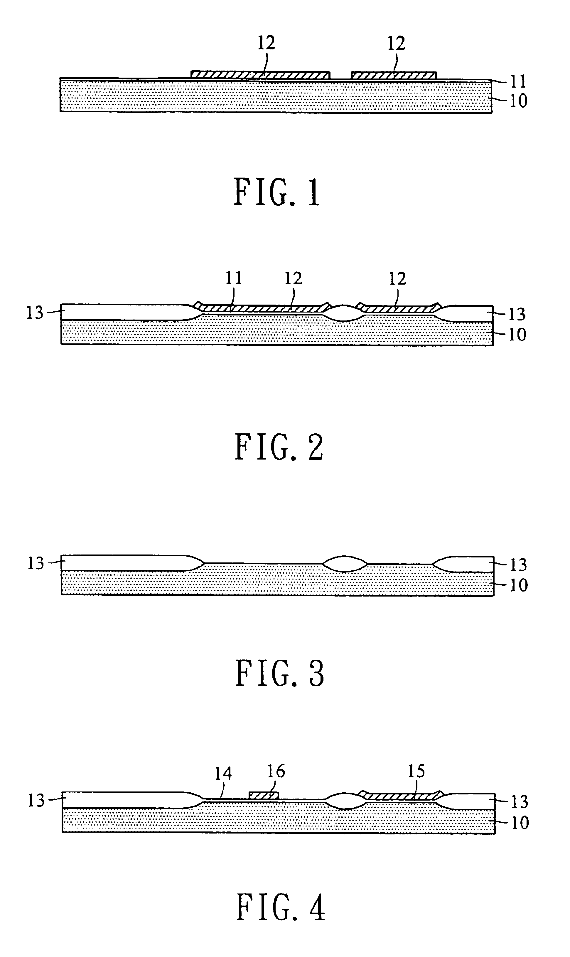
With reference to FIGS. 1 to 7, we use the n-channel metal oxide semiconductor field effect transistor (nMOSFET) as an example to explain the procedure of an embodiment of the invention. First, a silicon substrate is performed with the process of local oxidation of silicon (LOCOS), forming a field oxide (FOX) and defining out an active region and a body-contact active region. As shown in FIG. 1, the silicon substrate 10 is oxidized to form a stress buffer oxide 11. It is further deposited with a silicon nitride 12 using the chemical vapor deposition (CVD) method. After lithography and etching steps, the active region and the body-contact active region are defined on the silicon nitride 12. As shown in FIG. 2, a thick FOX 13 is subsequently formed using high-temperature wet oxidation. Finally, the stress buffer oxide 11 and the silicon nitride 12 are removed, forming the structure in FIG. 3.

Secondly, the gate is defined and the active region is doped to form a drain and a source. For...


PUM


Abstract

A MOSFET and the method for fabricating them are disclosed to make the inkjet head chips. The MOSFET has the scaled-down junction formation for the source and drain. Using a lower temperature process and interlayer dielectric, the source and drain dopants can not be diffused deeply due to high-temperature driver-in. The contact holes of the drain are provided with plugs of refractory material to avoid spiking between the metal and silicon. This achieves the requirement of high-density devices on the print head chip.

Description

BACKGROUND OF THE INVENTION1. Field of InventionThe invention relates to a MOSFET and the method for manufacturing them. In particular, it relates to a MOSFET for ink-jet heads and the associated manufacturing method.2. Related ArtThe inkjet printer ejects ink droplets on a printing medium to form desired texts or pictures. The size, shape, material, density, and positioning of the produced ink droplets are important factors that will affect the printing quality. The smaller the ink droplet size is, the higher printing resolution one can achieve. However, under normal conditions, the printing speed is also sacrificed. In order to promote the printing speed and resolution, the number of nozzles on the print head chip is the substantial solution.To achieve this objective, driving devices with switch and active characteristics such as transistors and the ink droplet actuators are often integrated into a single inkjet print head chip. The number of cartridge contact points X and the num...

Claims


Application Information

Patent Timeline
IPC IPC(8): B41J2/14H01L21/02H01L29/66H01L29/78H01L21/324H01L27/06
CPCB41J2/14129H01L29/78H01L21/324H01L27/0629B41J2002/14387B41J2202/13
Inventor LIU, CHIEN-HUNGLIOU, JIAN-CHIUNCHEN, CHUN-JUNGHU, JE-PING
Owner INTELLECTUAL VENTURES II
Learn More