Semiconductor laser device having InGaAs compressive-strain active layer, GaAsP tensile-strain barrier layers, and InGaP optical waveguide layers
a laser device and active layer technology, applied in semiconductor lasers, applications, instruments, etc., can solve the problems of affecting the effect and increasing the probability of asymmetric tensile strength
- Summary
- Abstract
- Description
- Claims
- Application Information
AI Technical Summary
Benefits of technology
Problems solved by technology
Method used
Image
Examples
first embodiment
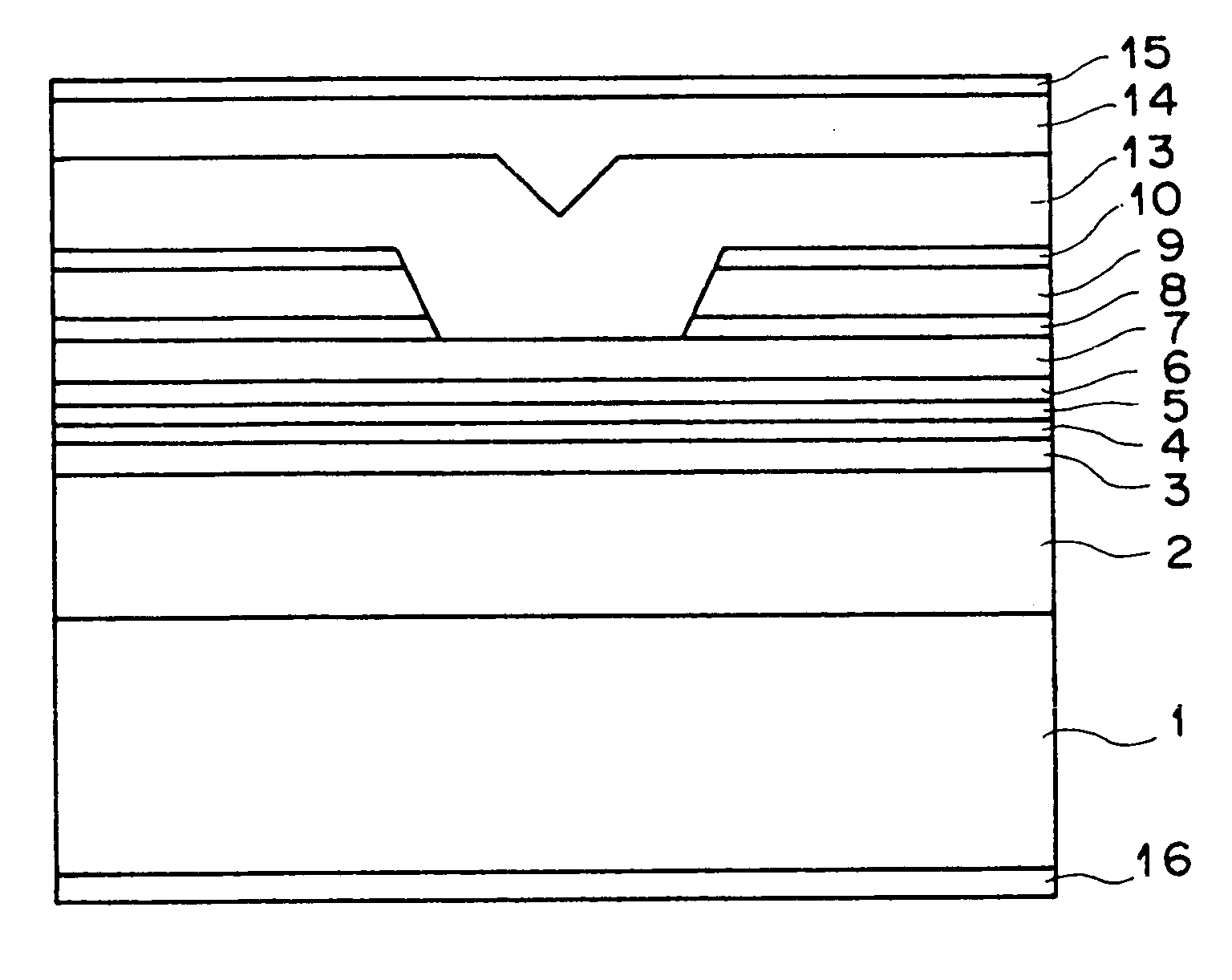
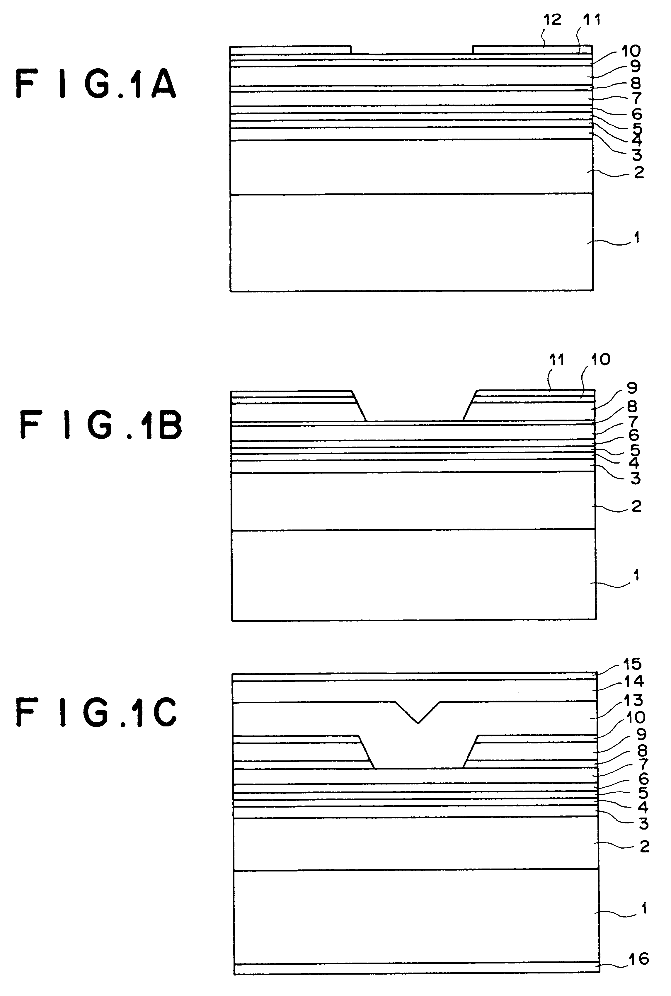
FIGS. 1A to 1C show cross sections of the representative stages in the process for producing a semiconductor laser device according to the first embodiment of the present invention.
First, as illustrated in FIG. 1A, an n-type Al.sub.z1 Ga.sub.1-z1 As lower cladding layer 2 (0.6.ltoreq.z1.ltoreq.0.8), an n-type or i-type (intrinsic) In.sub.0.49 Ga.sub.0.51 P lower optical waveguide layer 3, an In.sub.x2 Ga.sub.1-x2 As.sub.1-y2 P.sub.1-y2 tensile-strain barrier layer 4 (0.ltoreq.x2<0.49y2 and 0
second embodiment
FIG. 3 is a cross-sectional view of a semiconductor laser device according to the second embodiment of the present invention.
First, as illustrated in FIG. 3, an n-type Al.sub.z1 Ga.sub.1-z1 As lower cladding layer 22 (0.6.ltoreq.z1.ltoreq.0.8), an n-type or i-type (intrinsic) In.sub.0.49 Ga.sub.0.51 P lower optical waveguide layer 23, an In.sub.x2 Ga.sub.1-x2 As.sub.1-y2 P.sub.1-y2 tensile-strain barrier layer 24 (0.ltoreq.x2<0.49y2 and 0
third embodiment
FIG. 4 is a cross-sectional view of a semiconductor laser device according to the third embodiment of the present invention.
First, as illustrated in FIG. 4, an n-type Al.sub.z1 Ga.sub.1-z1 As lower cladding layer 42 (0.6.ltoreq.z1.ltoreq.0.8), an n-type or i-type (intrinsic) In.sub.0.49 Ga.sub.0.51 P lower optical waveguide layer 43, a GaAs.sub.1-y2 P.sub.y2 tensile-strain barrier layer 44 (0<y2.ltoreq.0.4), an In.sub.x3 Ga.sub.1-x3 As.sub.1-y3 P.sub.y3 compressive-strain quantum-well active layer 45 (0<x3.ltoreq.0.4, 0.ltoreq.y3.ltoreq.0.1), a GaAs.sub.1-y2 P.sub.y2 tensile-strain barrier layer 46, a p-type or i-type In.sub.0.49 Ga.sub.0.51 P upper optical waveguide layer 47, a p-type Al.sub.z1 Ga.sub.1-z1 As first upper cladding layer 48, a p-type In.sub.0.49 Ga.sub.0.51 P etching stop layer 49 having a thickness of about 10 nm, a p-type Al.sub.z1 Ga.sub.1-z1 As second upper cladding layer 50, and a p-type GaAs contact layer 51 are formed on an n-type GaAs substrate 41 by organome...
PUM
 Abstract
Description
Claims
Application Information
 - R&D
- Intellectual Property
- Life Sciences
- Materials
- Tech Scout
- Unparalleled Data Quality
- Higher Quality Content
- 60% Fewer Hallucinations
Browse by: Latest US Patents, China's latest patents, Technical Efficacy Thesaurus, Application Domain, Technology Topic, Popular Technical Reports.
© 2025 PatSnap. All rights reserved.Legal|Privacy policy|Modern Slavery Act Transparency Statement|Sitemap|About US| Contact US: help@patsnap.com


