Conductive adhesive with conductive particles, mounting structure, liquid crystal device and electronic device using the same

Inactive Publication Date: 2002-03-12
BOE TECH GRP CO LTD
View PDF16 Cites 28 Cited by
  • Summary
  • Abstract
  • Description
  • Claims
  • Application Information

AI Technical Summary

Benefits of technology

Furthermore, because the cores of the respective conductive particles contained in the conductive adhesive are formed using a synthetic resin having a high thermal deformation temperature, the conductive adhesive has high heat resistance. As a result, the conductive adhesive can withstand a solder reflow process in which the entire objects to be soldered are placed in a high temperature furnace. Therefore, it becomes possible to solder a chip component such as a capacitor to a base substrate by means of solder reflow processing after mounting a semiconductor chip on the base substrate using the conductive adhesive.
2. In the conductive adhesive described above, the synthetic resin forming the cores preferably has a thermal deformation temperature (18.6 kg / cm.sup.2) equal to or higher than 120.degree. C. as measured according to the measuring method defined in the ASTM (American Society of Testing Materials) standard D648. This allows the conductive adhesive to have higher heat resistance which ensures that the conductive adhesive withstands solder reflow processing.
If this mounting structure is employed, it is possible to first mount a semiconductor chip on a base substrate using the conductive adhesive and then mount a chip component on the base substrate by means of solder reflow processing. Thus, the mounting structure is stable and has a high reliability.
In this method of producing a mounting structure, because the cores of the respective conductive particles contained in the conductive adhesive are formed using a synthetic resin having a high thermal deformation temperature, the conductive adhesive has high heat resistance. Therefore, when a chip component such as a capacitor is soldered to a base substrate by means of solder reflow processing after mounting a semiconductor chip on the base substrate using the conductive adhesive, the conductive adhesive can withstand exposure to a high temperature during the soldering process.

Problems solved by technology

The conventional conductive adhesives such as an ACF used to mount a semiconductor chip include conductive particles formed of a synthesis resin such as polyester which is poor in heat resistance.
Therefore, it is impossible to perform solder reflow processing after mounting a semiconductor chip on the base substrate using a conventional conductive adhesive.
This results in suppression of occurrence of failures compared to the case where the mounting process using the conductive adhesive is performed after completion of the mounting process using the solder reflow technique.

Method used


Image

  • Conductive adhesive with conductive particles, mounting structure, liquid crystal device and electronic device using the same
  • Conductive adhesive with conductive particles, mounting structure, liquid crystal device and electronic device using the same
  • Conductive adhesive with conductive particles, mounting structure, liquid crystal device and electronic device using the same

Examples


second embodiment

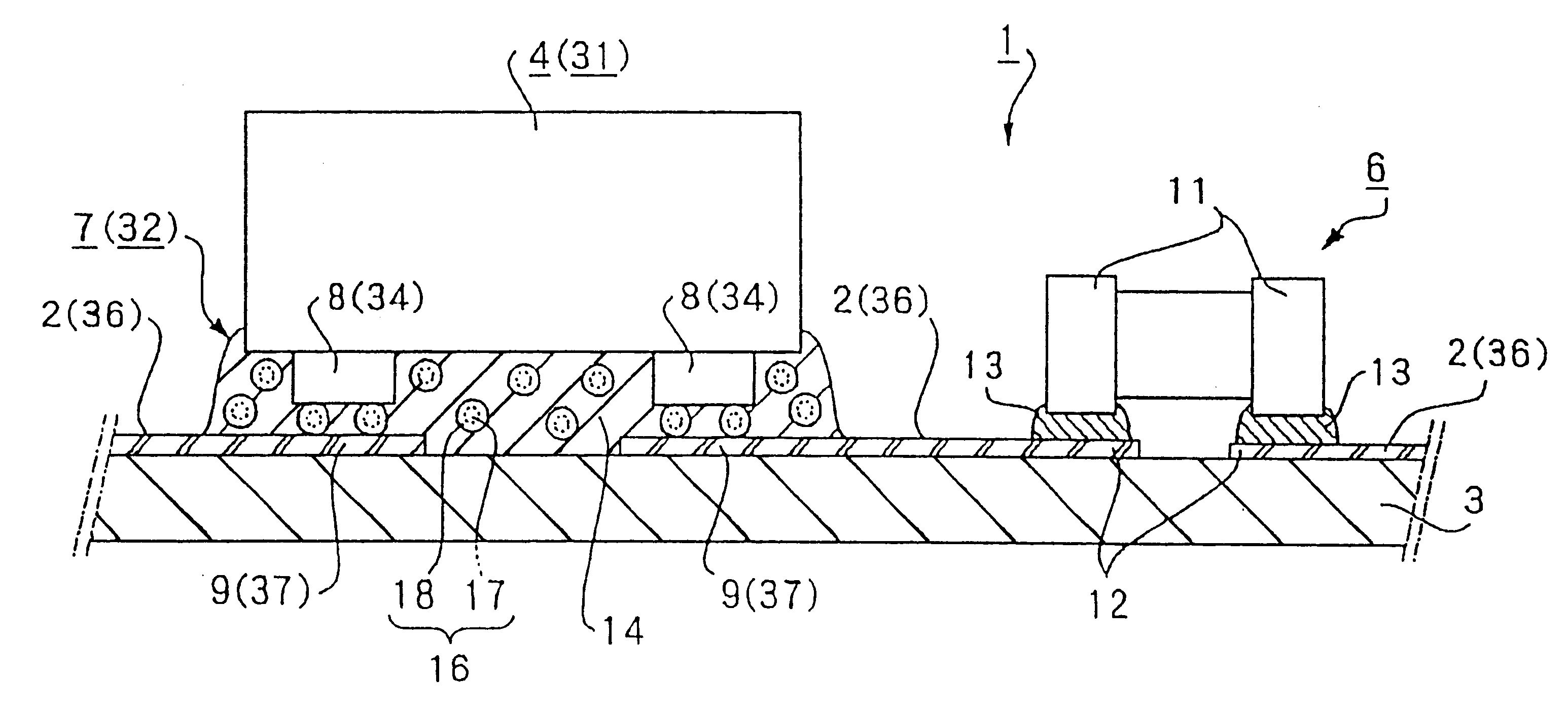
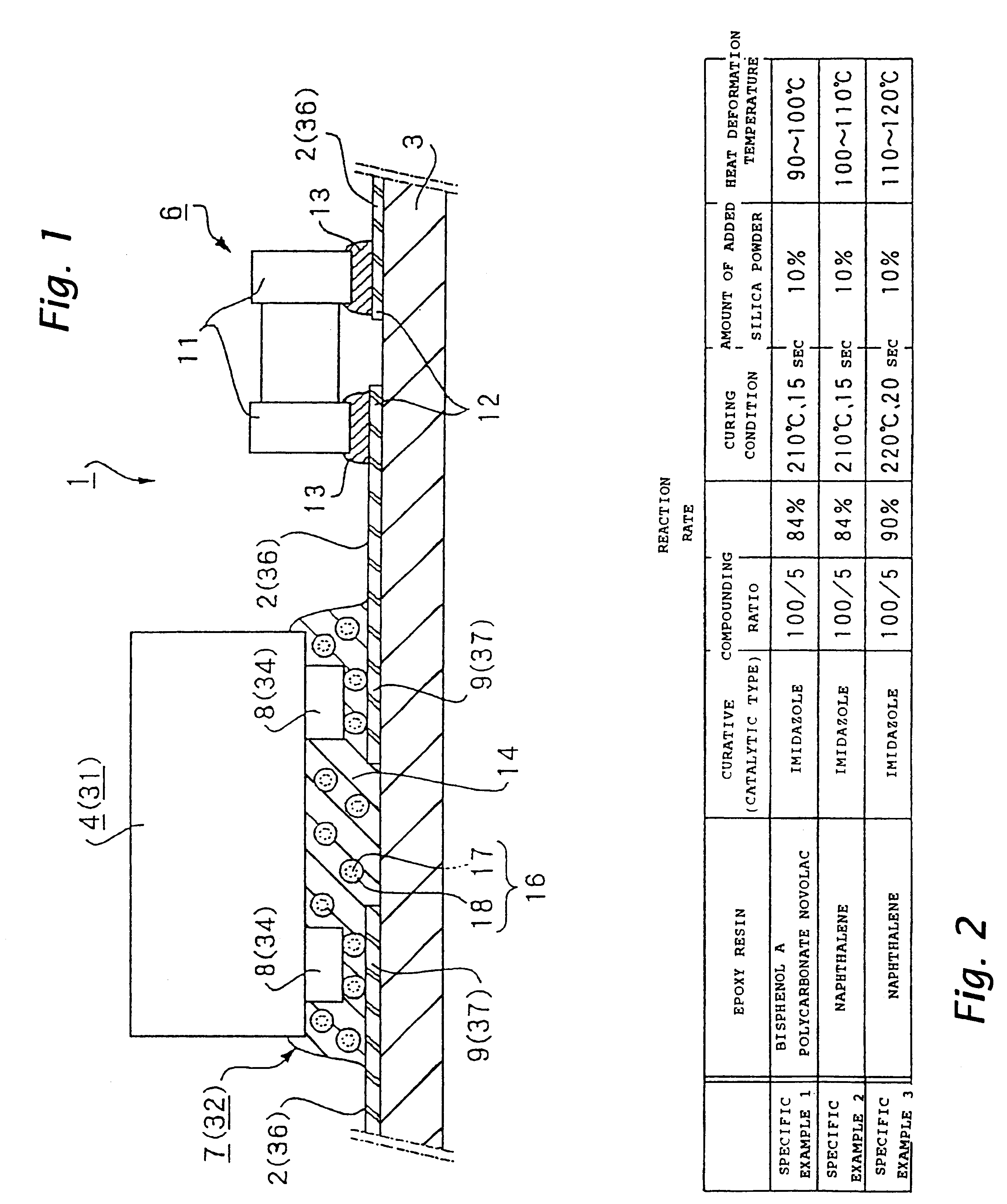
FIG. 7 illustrates an embodiment of a liquid crystal device according to the present invention. The liquid crystal device 21 shown in FIG. 7 is formed by connecting a mounting structure 23 to a liquid crystal panel 22. An illuminating device such as a backlight and other associated devices are also connected to the liquid crystal panel 22 as required.

The liquid crystal panel 22 includes a pair of substrates 26a and 26b connected to each other via a sealing member 24. A liquid crystal is sealed in a cell gap formed between the substrates 26a and 26b. The substrates 26a and 26b are generally formed of a transparent material such as glass or synthetic resin. A polarizer 28 is secured to the outer surface of each substrate 26a and 26b.

Electrodes 27a are formed on the inner surface of one substrate 26a, and electrodes 27b are formed on the inner surface of the other substrate 27b. These electrodes may be formed in the shape of stripes, characters, numerals, or other proper patterns. The ...

third embodiment

FIG. 9 illustrates a portable telephone which is an embodiment of an electronic device according to the present invention. The portable telephone 40 comprises an antenna 41, a loudspeaker 42, a liquid crystal device 21, key switches 43, a microphone 44, etc., wherein these components are disposed in a case 46. In the inside of the case 46, there is also provided a control circuit board 47 on which a control circuit for controlling the above-described components is disposed. The liquid crystal device 21 described above with reference to FIG. 7 may be employed herein as the liquid crystal device 21.

In this portable telephone 40, signals input via the microphone 44 or key switches 43 and a signal received via the antenna 41 are applied to the control circuit on the control circuit board 47. According to the input data, the control circuit displays an image such as a numeral, a character, or a graphical pattern in the display area of the liquid crystal device 21. Then the data is transm...


PUM


Abstract

A conductive adhesive which can withstand exposure to high temperature during a solder reflow process comprises an adhesive resin and a plurality of conductive particles mixed in the adhesive resin. The conductive particles each include a core formed of a synthetic resin and a conductive material coated around the core. The cores are each formed of a material having a thermal deformation temperature higher than that of the adhesive resin, and more preferably formed of a material having a thermal deformation temperature (18.6 kg / cm2) higher than 120° C. as measured according to the measuring method defined in the ASTM standard D648, and still more preferably formed of a material selected from the group consisting of polyphenylene oxide, polysulfone, polycarbonate, polyacetal, and polyethylene terephthalate.

Description

1. Field of the InventionThe present invention relates to a conductive adhesive used to mount an electronic component on a substrate or the like, and more particularly, to a conductive adhesive comprising an adhesive resin and a plurality of conductive particles mixed in the adhesive resin. The present invention also relates to a mounting structure formed using such a conductive adhesive. The present invention also relates to a liquid crystal device formed using such a mounting structure. The present invention also relates to an electronic device formed using such a liquid crystal device. The present invention also relates to a method of producing a mounting structure, a liquid crystal device, and an electronic device.2. Description of the Related ArtLiquid crystal devices are widely used in various electronic devices such as a portable telephone, a portable electronic terminal, etc. In many cases, liquid crystal devices are used to display information in the form of a character, a ...

Claims


Application Information

Patent Timeline
IPC IPC(8): G02F1/13H01L21/02H01L21/60H05K3/32H05K3/34H05K1/18C09J9/02C09J201/00H01L21/52
CPCG02F1/13452H01L24/29H01L24/83H05K3/323H01L2224/29101H01L2924/0665H01L2924/014H01L2924/01023H01L2924/01006H01L2224/2919H05K2201/10674H05K2201/0233H05K2201/0221H01L2224/16225H01L2224/29399H01L2224/73204H01L2224/8319H01L2224/838H01L2924/01004H01L2924/01005H01L2924/01013H01L2924/01029H01L2924/01033H01L2924/01049H01L2924/0105H01L2924/01078H01L2924/0781H01L2924/14H01L2924/19041H01L2924/19043H01L2924/19105H05K1/189H05K3/341H01L2924/00H01L2924/3512H01L2924/00014H01L2924/181H01L2224/0401C09J9/02
Inventor UCHIYAMA, KENJI
Owner BOE TECH GRP CO LTD
Why Eureka
Try Eureka