Ferroelectric dielectric for integrated circuit applications at microwave frequencies

Inactive Publication Date: 2000-11-14
NORTEL NETWORKS LTD
View PDF3 Cites 22 Cited by
  • Summary
  • Abstract
  • Description
  • Claims
  • Application Information

AI Technical Summary

Benefits of technology

Thus, the present invention seeks to provide a ferroelectric dielectric for an integrated circuit which avoids or reduces the above mentioned problems, with particular application to formation of ferroelectric capacitors for applications at microwave frequencies.
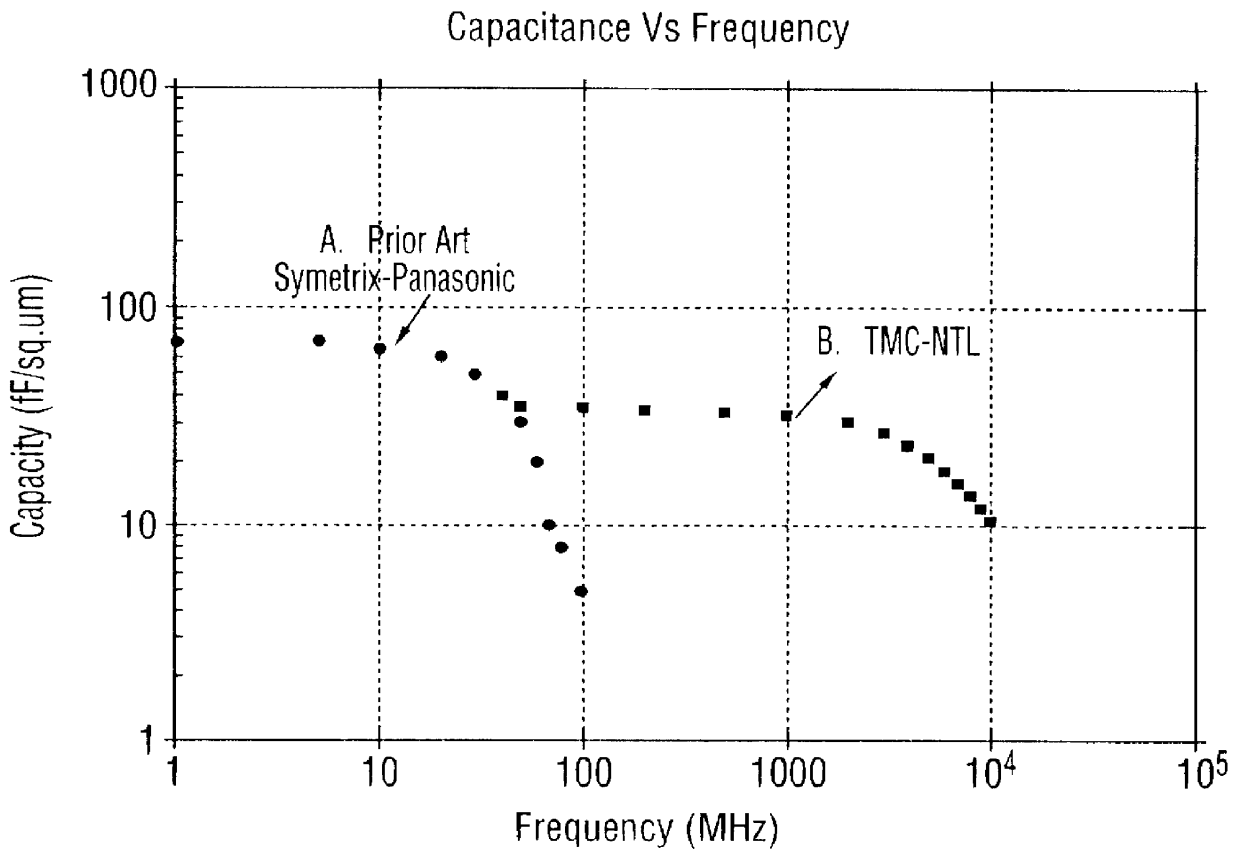
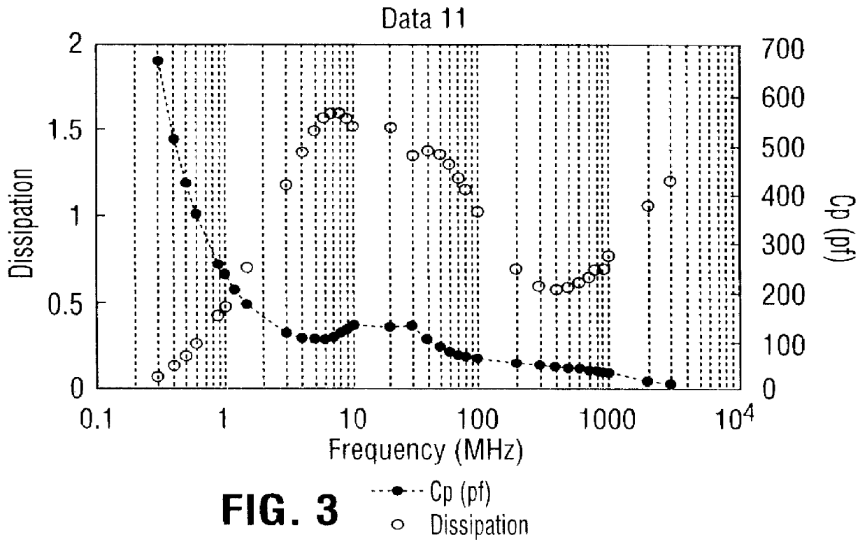
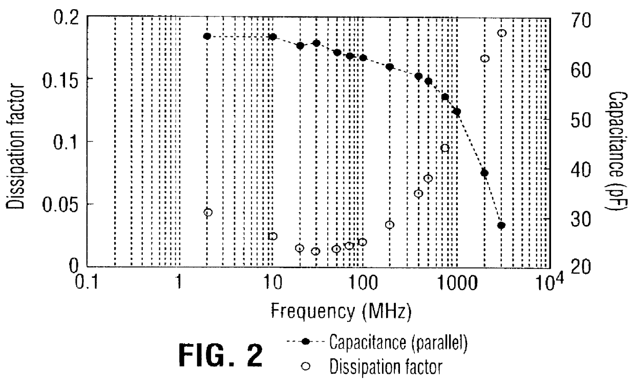
In preparing PZT films having high frequency performance above 1 GHz, a low temperature method was employed, for example a sol-gel process, comprising annealing, by rapid thermal processing, in an oxygen and ozone containing atmosphere, and preferably in the presence of water vapour. In addition to providing PZT films with high dielectric constant >300 and low film stress, it was discovered that the frequency response of the PZT was extended into the GHz range relative to the roll-off in dielectric constant which occurs at about 100 MHz in bulk ceramic PZT. Consequently, the usefulness of this material as a ferroelectric dielectric, is extended for use, e.g. for capacitors for integrated circuits operable at microwave frequencies. In other applications, these fine grained polycrystalline PZT may be used for high frequency surface acoustic wave (SAW) devices having low mechanical loss.
It is believed that other low temperature methods of forming PZT and doped PZT, for example by CVD, MOCVD, laser ablation, ion beam sputtering, may also be used to provide high frequency ferroelectric PZT material having small grain size PZT, having a roll off frequency exceeding 1 GHz. In defining fine grained in this context, while small grain sizes .about.10 nm are preferred, grain sizes above 20 nm can be expected to provided improved response in the high frequency region compared to bulk PZT. The upper limit to the useful grain size to obtain a roll off frequency above 1 GHz is likely to be less than 1 .mu.m, but substrate clamping in thin films, discussed below, may significantly affect the dielectric dispersion relative to bulk samples. In thin films, extra clamping effects from the substrate may extend the useful grain size to .about.1 .mu.m or beyond.
Thus the present invention provides a ferroelectric dielectric material, a ferroelectric capacitor for an integrated circuit structure, and a method of formation thereof, which overcome or reduce some of the above mentioned problems.

Problems solved by technology

These memory elements also consume low power, are dense and exhibit radiation hardness.
Integration of ferroelectric materials with monolithic integrated circuits brings challenges including the selection of compatible materials for bottom and top electrodes, and for barrier layers and capping layers, to avoid or control contamination problems.
They concluded that this material was not useful as a capacitor material at high frequencies.
Nevertheless, at low frequencies, BST has a lower dielectric constant that PZT, and BST typically requires higher processing temperatures.

Method used


Image

  • Ferroelectric dielectric for integrated circuit applications at microwave frequencies
  • Ferroelectric dielectric for integrated circuit applications at microwave frequencies
  • Ferroelectric dielectric for integrated circuit applications at microwave frequencies

Examples


Embodiment Construction

In a method of forming a ferroelectric dielectric for a capacitor structure according to a first embodiment of the present invention, a ferroelectric capacitor structure was formed on an integrated circuit substrate comprising a semiconductor silicon wafer. A bottom electrode of a capacitor was defined on the substrate. The bottom electrode comprises a single conductive layer, or alternatively comprises a multilayer structure including a barrier layer and an adhesion layer. In the present example a bottom electrode was formed from sputtered platinum. A layer of lead zirconate titanate (PZT) was then formed on the bottom electrode as described in the above mentioned copending U.S. patent application Ser. No. 08-348848, using a known spin-on liquid process to apply to the substrate a metallorganic sol-gel precursor comprising constituents of the ferroelectric material, i.e. an inorganic lead compound, and zirconium and titanium alkoxides in the desired proportions, e.g. to provide a 4...


PUM

PropertyMeasurementUnit
Grain sizeaaaaaaaaaa
Angleaaaaaaaaaa
Frequencyaaaaaaaaaa

Abstract

A ferroelectric dielectric for microwave applications is provided comprising a polycrystalline perovskite phase of lead zirconate titanate dielectric material. Small grain size material is provided by a low temperature process, by a rapid thermal annealing process. A layer of amorphous ferroelectric precursor material is deposited and annealed in an oxygen containing atmosphere in the presence of water vapor, preferably with the addition of a few percent of ozone, and at a temperature of less than 500.degree. C. Advantageously, the method provides for formation of a ferroelectric material comprising lead zirconate titanate with a grain size less than 20 nm, with low film stress, high dielectric constant and low leakage current, which has excellent ferroelectric characteristics up to 10 GHz. This material has applications for capacitors, as filters, decoupling, coupling, and bypass elements and also for high frequency surface acoustic wave devices.

Description

FIELD OF THE INVENTIONThis invention relates to ferroelectric dielectric for integrated circuit applications at microwave frequencies, and with particular application to ferroelectric capacitors and memory cells.BACKGROUND OF THE INVENTIONIn recent years, the use of the ferroelectric materials for random access memory (RAM) elements has reached commercial applications in the semiconductor industry. Ferroelectric dielectrics typically have very high dielectric constants .about.500, which make these materials attractive as dielectrics for capacitors with high charge storage capacity. Ferroelectric memory elements are non-volatile, and programmable with low voltage, e.g. less than 5V. Other advantages include fast access times (<40 ns), and robustness with respect to virtually unlimited numbers of read and write cycles. These memory elements also consume low power, are dense and exhibit radiation hardness.Ferroelectric materials which have allowed this breakthrough in integrated cir...

Claims


Application Information

Patent Timeline
IPC IPC(8): H01G7/00H01G7/06
CPCH01G7/06C04B2235/658C04B2235/6588C04B2235/663C04B35/491C04B2235/768
Inventor CHIVUKULA, VASANTALEUNG, PAK K.
Owner NORTEL NETWORKS LTD
Why Eureka
Try Eureka