
Material for forming organic film, method for forming organic film, patterning process, and compound

a technology of organic film and patterning process, which is applied in the field of organic film material, organic film method, patterning process, compound, etc., can solve the problem of not having a dry etching method capable of providing absolute etching selectivity, the aspect ratio of the material becomes so large, and the pattern collapse occurs consequently. , to achieve the effect of excellent adhesive force to the substrate, high filling property, and high planarizing property

Active Publication Date: 2021-06-17
SHIN ETSU CHEM IND CO LTD
View PDF4 Cites 1 Cited by
  • Summary
  • Abstract
  • Description
  • Claims
  • Application Information

AI Technical Summary

Benefits of technology

The present invention provides a compound that can be used to form an organic film with high filling, planarizing, and adhesive properties to a substrate. The material can be used in manufacturing semiconductor devices and resist underlayer films. The inventive methods for forming an organic film can create a flat, well-cured film on a substrate and can accurately form fine patterns in a substrate.

Problems solved by technology

In addition, if the photoresist film is pattern-developed by using a developer, what is called an aspect ratio thereof becomes so large that pattern collapse occurs consequently.
In practice, however, there is no dry etching method capable of providing an absolute etching selectivity between the photoresist film and the substrate to be processed.
Thus, the resist film is also damaged and collapses during the substrate processing, and the resist pattern cannot be precisely transferred to the substrate to be processed.
This shift actually accelerates the etching rate under these dry etching conditions, and recent photoresist compositions having high resolution tend to have rather low etching resistance.
However, an organic film formed by this method contains many polyether polyol units, which are inferior in etching resistance.
Thus, this film has a markedly lowered etching resistance and is unsuitable for the three-layer resist underlayer film.
Nevertheless, this resist underlayer film material has a problem that the adhesiveness to a substrate is insufficient to meet the demands for cutting-edge devices.
Furthermore, although a CMP process is now generally used for global planarization in the semiconductor device manufacturing process, the organic film material is also expected to be used for the global planarizing method in place of the CMP process because CMP is costly.

Method used


Image

  • Material for forming organic film, method for forming organic film, patterning process, and compound
  • Material for forming organic film, method for forming organic film, patterning process, and compound
  • Material for forming organic film, method for forming organic film, patterning process, and compound

Examples


synthesis example 1

[Synthesis Example 1] Synthesis of Compound (A1)

[0300]

[0301]Under a nitrogen atmosphere, a homogeneous solution with an inner temperature of 100° C. was prepared from 20.0 g of Epoxy Compound (B1), 19.9 g of Phthalimide Compound (C1), and 200 g of 2-methoxy-1-propanol. Then, 1.00 g of benzyltriethylammonium chloride was added thereto and stirred for 12 hours with the inner temperature of 120° C. After cooling to room temperature, 300 ml of methyl isobutyl ketone was added, and washing was performed twice with 100 g of a 2% NaHCO3 aqueous solution and 100 g of a 3% nitric acid aqueous solution, and five times with 100 g of ultrapure water. The organic layer was evaporated under reduced pressure to dryness. Thus, Compound (A1) was obtained. The weight-average molecular weight (Mw) and dispersity (Mw / Mn) thereof was determined by GPC. The results were Mw=780 and Mw / Mn=1.02.

[Synthesis Examples 2 to 29] Synthesis of Compounds (A2) to (A29)

[0302]Compounds (A2) to (A29) as shown in Tables ...

example 1

ess and Filling Property Evaluations (Examples 1-1 to 1-32, Comparative Examples 1-1 to 1-4)

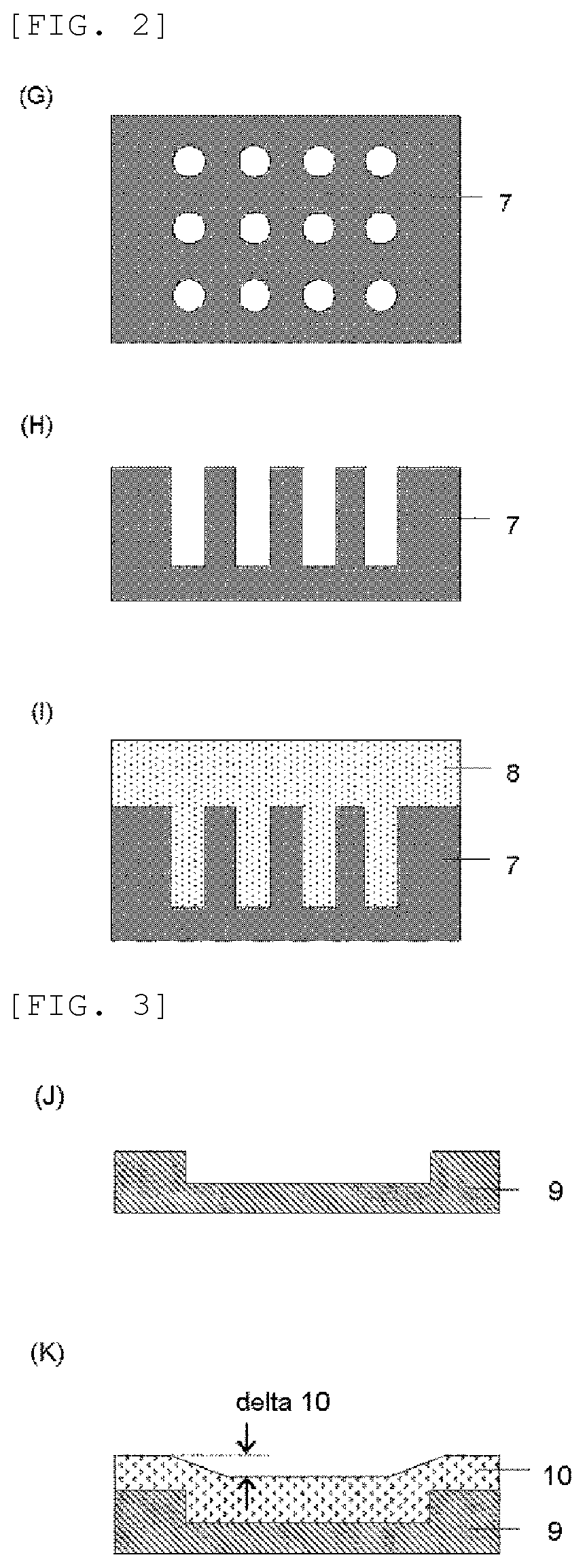
[0310]As shown in FIG. 2, the materials (UDL-1 to -32, Comparative Example UDL-1 to -4) for forming an organic film were each applied onto a SiO2 wafer substrate having a dense hole pattern (hole diameter: 0.16 μm, hole depth: 2.0 μm, distance between the centers of adjacent two holes: 0.32 μm), the SiO2 wafer substrate having been treated with hexamethyldisilazane (HMDS). The resultant was baked with a hot plate in the atmosphere under conditions shown in Tables 4-1 and 4-2. Thereby, an organic film 8 was formed. The substrate used was a base substrate 7 (SiO2 wafer substrate) having a dense hole pattern as shown in FIG. 2 (G) (top view) and (H) (sectional view). The sectional shapes of the resulting wafer substrates were observed with a scanning electron microscope (SEM) to check whether or not the holes were filled with the organic film without voids (space). Tables 4-1 and 4-2 show the re...

example 2

ng Property Evaluation (Examples 2-1 to 2-32, Comparative Examples 2-1 to 2-4)

[0312]The materials (UDL-1 to -32, Comparative Example UDL-1 to -4) for forming an organic film were each applied onto a base substrate 9 (SiO2 wafer substrate) having a giant isolated trench pattern (FIG. 3 (J), trench width: 10 μm, trench depth: 0.10 μm), and baked with a hot plate in the atmosphere under conditions shown in Tables 5-1 and 5-2. Then, a step (delta 10 in FIG. 3 (K)) between the trench portion and the non-trench portion of an organic film 10 was observed with an atomic force microscope (AFM) NX10 manufactured by Park systems Corp. Tables 5-1 and 5-2 show the results. In this evaluation, the smaller the step, the better the planarizing property. Note that, in this evaluation, a trench pattern having a depth of 0.10 μm was generally planarized using an organic film material having a film thickness of 200 nm. This is a severe evaluation condition to evaluate the planarizing property.

TABLE 5-1...


PUM

PropertyMeasurementUnit
boiling pointaaaaaaaaaa
temperatureaaaaaaaaaa

Abstract

The present invention provides a material for forming an organic film, containing a compound shown by the following general formula (1), and an organic solvent, where X represents an organic group having a valency of n1 and 2 to 50 carbon atoms, n1 represents an integer of 1 to 10, and R1 represents at least one or more of the following general formulae (2) to (4). This aims to provide an organic film material for forming an organic film that has all of high filling property, high planarizing property, and excellent adhesive force to a substrate.

Description

TECHNICAL FIELD[0001]The present invention relates to a material for forming an organic film, a method for forming an organic film, a patterning process, and a compound.BACKGROUND ART[0002]As LSIs advance toward higher integration and higher processing speed, miniaturization of pattern size is rapidly progressing. Along with this miniaturization, the lithography technology has achieved formation of fine patterns by shortening the wavelength of a light source and by selecting a proper resist composition corresponding to the shortened wavelength. The main factor of this achievement is a positive photoresist composition used as a monolayer. This monolayer positive photoresist composition allows a resist resin to have not only a skeleton that possesses etching resistance against dry etching with chlorine- or fluorine-based gas plasma, but also a resist mechanism that makes an exposed part soluble. Thereby, after a pattern is formed by dissolving the exposed part, a substrate to be proce...

Claims


Application Information

Patent Timeline
Patent Type & Authority Applications(United States)
IPC IPC(8): G03F7/11C08F26/06C09D139/04C07D209/48C07D403/14C07D487/04G03F7/09H01L21/027H01L21/033H01L21/768
CPCG03F7/11C08F26/06C09D139/04C07D209/48H01L21/76819C07D487/04G03F7/094H01L21/0273H01L21/0337C07D403/14G03F7/004G03F7/027C07D303/30C07D405/14C07C53/126C07C65/28C09D171/12C09D171/00H01L21/02118H01L21/0271G03F7/26H01L21/027H01L21/0276H01L21/0332
Inventor KORI, DAISUKENAKAHARA, TAKAYOSHIBIYAJIMA, YUSUKE
Owner SHIN ETSU CHEM IND CO LTD
Learn More