
Silicon carbide based field effect gas sensor for high temperature applications

a gas sensor and field effect technology, applied in the field of silicon carbide (sic) based field effect gas sensor, can solve the problems of incomplete combustion of fuel, incomplete oxidation of hydrocarbon species and co, and general emission of substances such as nitrogen oxides

Inactive Publication Date: 2018-01-11
VOLVO CAR CORP
View PDF4 Cites 212 Cited by
  • Summary
  • Abstract
  • Description
  • Claims
  • Application Information

AI Technical Summary

Benefits of technology

The present invention provides an improved SiC-based field effect gas sensor that can operate reliably in high-temperature and harsh environments. The use of a layer of electrically conducting metal oxide as a protective layer has been found to prevent oxidation of the underlying ohmic layer for a long time at higher temperatures. The protective layer also does not react with other layers, leaving them intact with retained properties. The thermal expansion mismatch of the protective layer with other passivation layers is small, which adds to its stability at extreme temperatures. The use of such protective layers allows the SiC-based field effect gas sensor to reliably operate at temperatures above 600°C without any degradation of the underlying layers.

Problems solved by technology

Combustion processes in e.g. internal combustion car engines, power plants, district heating plants, gas turbines, and domestic heating facilities generally lead to emissions of substances such as nitrogen oxides, hydrocarbons and carbon monoxide (CO), especially if the processes are neither optimized nor controlled.
Deficiency or too much of excess air in the combustion processes lead to either incomplete combustion of the fuel or slow combustion kinetics, with the result that incompletely oxidized hydrocarbon species and CO are left in the exhaust or flue gases.
The presently existing options regarding such monitoring and determination is however very limited due to the harsh conditions, e.g. high temperature, vibrations, and corrosive environments, encountered in the processes of interest.
Most solid-state gas sensors are either not able to operate under harsh conditions or suffer long-term stability problems.
As an example, in the special application of Exhaust Gas Recirculation (EGR), there is at present no existing satisfactory oxygen sensor for control of the exhaust recirculation (often referred to as an intake oxygen sensor).
Due to the special conditions prevailing in the engine intake compartment, any kind of sensors being subjected to e.g. condensed water, soot, and oil residues, the Universal Exhaust Gas Oxygen (UEGO) sensor currently in use for exhaust or flue gas oxygen concentration assessment does not withstand the conditions encountered and is not able to fulfil the requirements on reliability set by the automotive industry.
Resistive-type semiconducting metal oxide based sensors (commonly fabricated from materials like tin oxide-SnO2) generally also suffer from long-term stability issues under conditions prevailing for this particular as well as other exhaust / flue gas monitoring and combustion control applications, in addition to poor selectivity.
The various kinds of optical sensors that have been developed are quite expensive and suffer from undesired spatial fluctuations when directing the laser beam of the sensor to desired locations (also referred to as “beam wobble” or “pointing instability”), as well as long-term stability issues.
This sensor technology, however, suffers from substantial cross-sensitivity to ammonia, making direct, accurate measurements of downstream NOx concentrations challenging.
However, neither field effect gas sensors nor other kinds of discrete semiconductor devices or ICs based on SiC have yet found any commercial success for the really high temperature applications (>450° C.
), mainly due to reliability issues.
In view of long-term reliable high temperature device operation, including sensors, general critical issues are e.g. matching of the temperature expansion and heat conductivity of the materials combined in the device as well as the high temperature (and especially temperature cycling) endurance of electrical leads, contacts, and protective passivation / encapsulation materials.
For low voltage high temperature devices the most prominent reasons behind long-term degradation result from die attachment and contact failure, the latter due to the degradation of metallizations for protective capping and / or passivation layers of electrical ohmic contacts as well as electrical leads / bond pad stacks and the subsequent restructuring / oxidation of the ohmic contacts when oxygen diffuses through the metal capping layers.
Although measures have been taken to improve the reliability of SiC-based field effect gas sensors and other devices for high temperature applications, problems with the structural integrity and / or oxidation of conductive (ohmic) contact and protective / passivation layers remain for operation temperatures of about 500° C. and above, so far preventing their use in a number of the above mentioned applications.
As previously discussed, for a number of the parameters desired to monitor, one example being ammonia concentration downstream of the SCR catalyst, there are no viable commercially available sensor options existing at the moment.
There are also doubts whether the sensor technology which exist today to monitor some of the other parameters, such as tailpipe-out concentration of nitrogen oxides, will be able to fulfil the accuracy requirements when emissions legislation in the near future will be made even tighter.

Method used


Image

  • Silicon carbide based field effect gas sensor for high temperature applications
  • Silicon carbide based field effect gas sensor for high temperature applications
  • Silicon carbide based field effect gas sensor for high temperature applications

Examples


Embodiment Construction

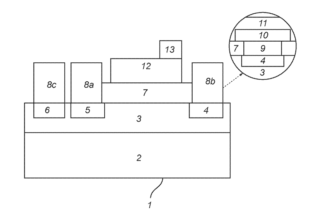
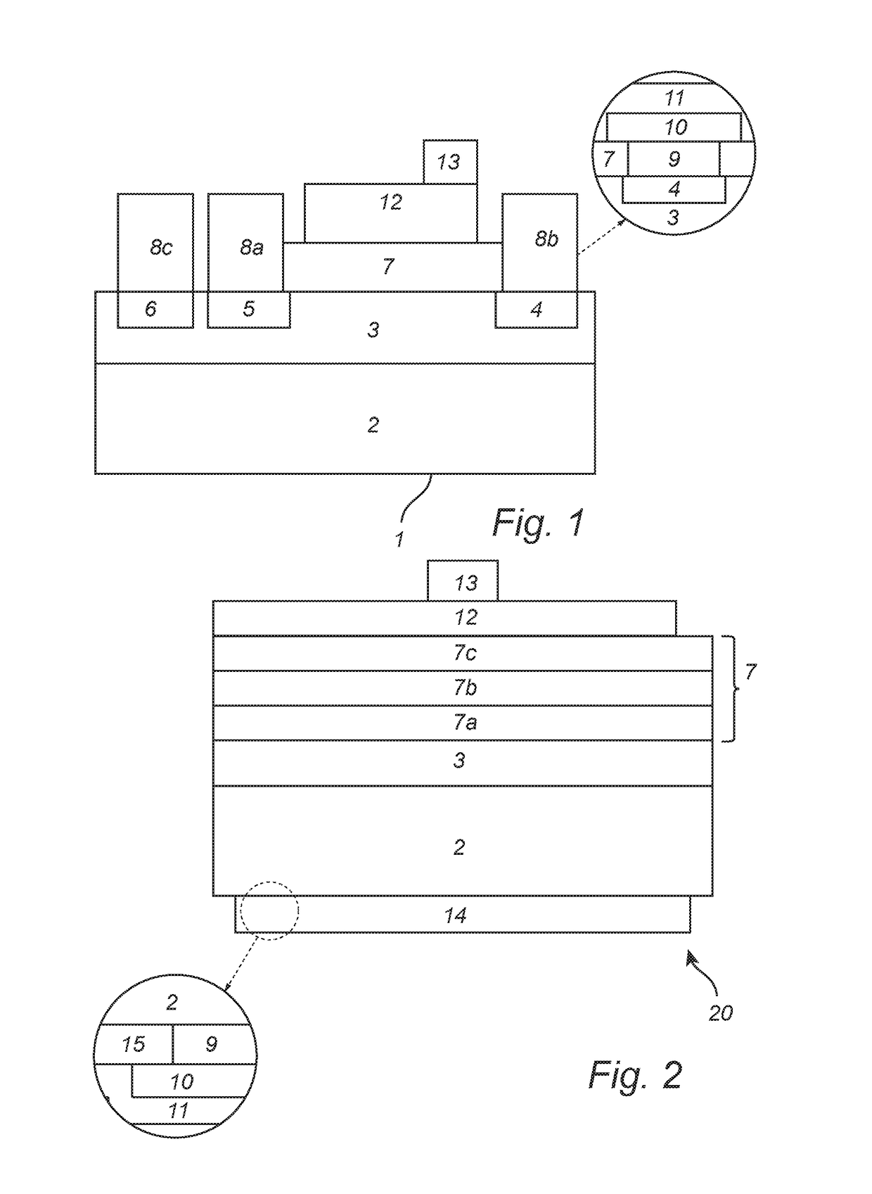
[0044]FIG. 1 displays an example of a field effect gas sensor of the MOSFET / MISFET type 1 according to an embodiment of the present disclosure. The field effect gas sensor of the MOSFET / MISFET type 1 comprises a semiconductor layer 2 of e.g. n-type doped SiC. On the semiconductor layer 2, an epilayer 3 (also of SiC), of p-type (doping concentration 5−1015 / cm3) is grown to a thickness of approximately 10 μm. In the epilayer, 3 doped regions are created e.g. by ion implantation to form a drain region 4 of n-type, a source region 5 of n-type and a substrate region 6 of p-type (doping concentration approximately −1020 / cm3). On top of the epilayer 3 an electron insulating layer 7 is grown, consisting of e.g. a thermally grown SiO2 layer to an approximate thickness of 500 Å, and an LPCVD deposited layer of silicon nitride (Si3N4) of approximate thickness 250 Å, which is densified to create a thin layer of silicon dioxide on top of the nitride, typically 50 Å.

[0045]Three contact structures...


PUM


Abstract

A field effect gas sensor, for detecting a presence of a gaseous substance in a gas mixture, the field effect gas sensor comprising: a SiC semiconductor structure; an electron insulating layer covering a first portion of the SiC semiconductor structure; a first contact structure at least partly separated from the SiC semiconductor structure by the electron insulating layer; and a second contact structure conductively connected to a second portion of the SiC semiconductor structure, wherein at least one of the electron insulating layer and the first contact structure is configured to interact with the gaseous substance to change an electrical property of the SiC semiconductor structure; and wherein the second contact structure comprises: an ohmic contact layer in direct contact with the second portion of the SiC semiconductor structure; and a barrier layer formed by an electrically conducting mid-transition-metal oxide covering the ohmic contact layer.

Description

RELATED APPLICATION[0001]This application claims priority under 35 U.S.C. §119 based on European Patent Application No. 16178557.1, filed Jul. 8, 2016, the disclosure of which is hereby incorporated by reference herein.FIELD OF THE INVENTION[0002]The present invention relates to a silicon carbide (SiC) based field effect gas sensor and to a method of manufacturing such a gas sensor.BACKGROUND OF THE INVENTION[0003]Wide band gap semiconductor materials, such as silicon carbide (SiC), have recently attracted a lot of interest for the development of devices and electronics for high temperature and also high power applications. One example of current interest concerns the demands for power electronics to connect grid-level energy storage facilities to a power grid largely based on renewable, intermittent energy sources, such as wind and waves. The wide band gap (3.2 eV in the case of 4H—SiC, which is the most common polytype for device fabrication) permits operation at temperatures high...

Claims


Application Information

Patent Timeline
IPC IPC(8): G01N27/414H01L21/04H01L29/16H01L29/45
CPCG01N27/4141H01L21/0485H01L29/45H01L29/1608
Inventor ANDERSSON, MIKEFASHANDI, HOSSEIN
Owner VOLVO CAR CORP
Learn More